Display device and preparation method thereof

一种显示装置、显示区的技术,应用在半导体/固态器件制造、半导体器件、电气元件等方向,能够解决外部水氧渗透、有机发光材料功能退化、影响显示装置寿命等问题,达到延长生命周期、增强密封性能的效果

Active Publication Date: 2020-04-10
SHENZHEN CHINA STAR OPTOELECTRONICS SEMICON DISPLAY TECH CO LTD
View PDF6 Cites 8 Cited by
  • Summary
  • Abstract
  • Description
  • Claims
  • Application Information

AI Technical Summary

Problems solved by technology

[0005] The object of the present invention is to provide a display device and its preparation method to solve the poor encapsulation effect of light-emitting elements in the prior art, which easily causes external water and oxygen to penetrate into the organic light-emitting layer, degrades the function of the organic light-emitting material, and affects Display technical issues of device lifespan

Method used


Image

  • Display device and preparation method thereof
  • Display device and preparation method thereof
  • Display device and preparation method thereof

Examples


Embodiment 1

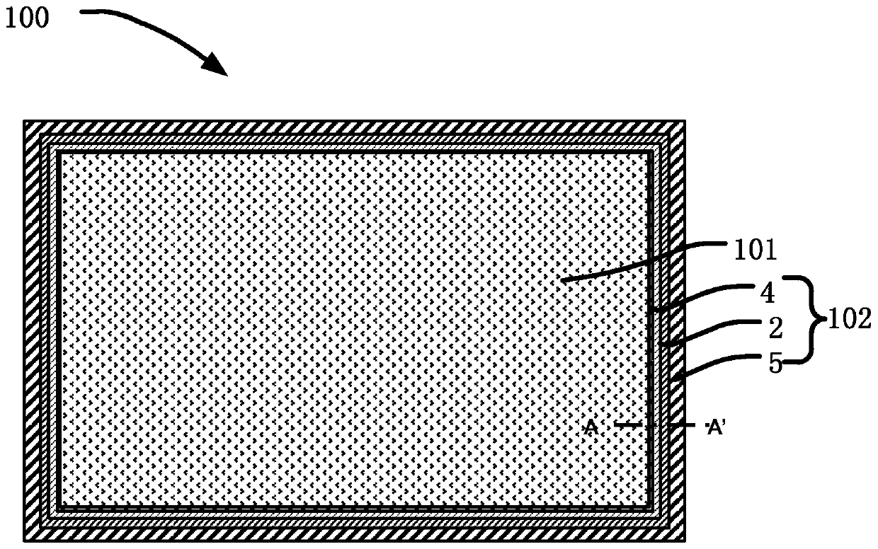
[0035] Such as Figure 1~2 As shown, this embodiment provides a display device 100 , including a display area 101 and a non-display area 102 , and the non-display area 102 surrounds the display area 101 .

[0036] Such as figure 2 As shown, the display device 100 further includes a thin film transistor structure layer 1 , a ring metal layer 2 , a light emitting layer 3 , a first electrode 4 and an encapsulation layer 5 . The annular metal layer 2 is disposed in the thin film transistor structure layer 1 , and the annular metal layer 2 is located in the non-display area 102 and surrounds the display area 101 . The light emitting layer 3 is disposed on the thin film transistor structure layer 1 and located in the display area 101 . The first electrode 4 is disposed above the light-emitting layer 3 , extends from the display area 101 to the surface of the ring-shaped metal layer 2 in the non-display area 102 , and completely covers the surface of the ring-shaped metal layer 2 ...

Embodiment 2

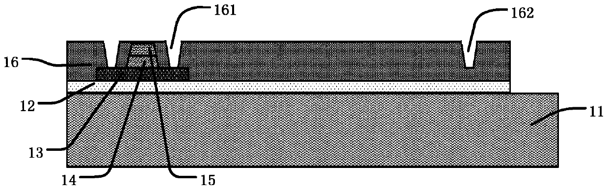
[0083] This embodiment provides a display device and a manufacturing method thereof, which includes most of the technical features of Embodiment 1, the difference being that the first annular metal layer is disposed on the dielectric layer and protrudes from the blunt The layer can also provide a good contact surface for the first electrode, so that the first electrode is fixedly connected to the annular metal layer; second, the display device includes at least one first groove, from which The pixel definition layer extends to the surface of the passivation layer to cut off the water vapor transmission path; thirdly, the packaging layer includes a water-blocking and moisture-absorbing adhesive layer and a metal foil instead of a cover layer and a cover plate, and can also Realize the effect of blocking water and oxygen.

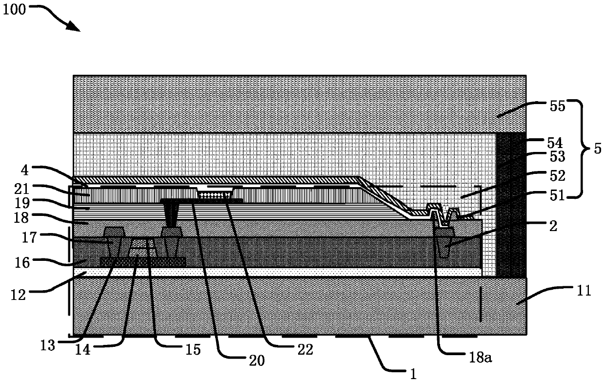
[0084] Such as Figure 5 As shown, the display device 100 further includes a thin film transistor structure layer 1 , a ring metal layer 2 , a light emittin...


PUM


Abstract

The invention discloses a display device and a preparation method thereof. The display device comprises a display area and a non-display area, and the non-display area surrounds the display area; thedisplay device further comprises a thin film transistor structure layer, an annular metal layer, a light-emitting layer and a first electrode. The display device and the preparation method thereof have the technical effects that the first electrode extends from the display area to the surface of the annular metal layer of the non-display area and completely covers the surface of the annular metallayer, so that metal-to-metal direct contact is formed, and the capacity of an interface for blocking water and oxygen is improved; and when moisture invades laterally, a compact oxidation film is formed on the surface of the first electrode to play a blocking role, and meanwhile, a bulge is formed at the position, corresponding to the annular metal layer, of a passivation layer and plays a role of a small dam to block the moisture layer by layer, so that the sealing performance of a light-emitting element is enhanced, and the life cycle is prolonged.

Description

technical field [0001] The present invention relates to the field of display technology, in particular to a display device and a preparation method thereof. Background technique [0002] Organic light emitting diodes (Oganic Light Emitting Diodes, OLED) display includes two electrodes and an organic light-emitting layer between the two, electrons and holes are respectively injected from the two electrodes into the organic light-emitting layer to form excitons, and the excitons release energy glow in the process. [0003] The above-mentioned organic light-emitting element is located on the substrate, and the material of the organic light-emitting layer is sensitive to moisture, oxygen and other external factors and deteriorates, which affects the display effect of the product. Therefore, it is particularly important to seal the light-emitting element. [0004] In large-size organic light-emitting display devices, there are currently two mainstream packaging technologies: the...

Claims


Application Information

Patent Timeline
Patent Type & Authority Applications(China)
IPC IPC(8): H01L51/52H01L27/32
CPCH10K59/12H10K50/82H10K50/84H10K59/1201H10K59/124H10K50/8423H10K50/846H10K50/8426H10K50/844H10K59/88H10K59/122H10K71/00
Inventor 杜彦英
Owner SHENZHEN CHINA STAR OPTOELECTRONICS SEMICON DISPLAY TECH CO LTD
Why Eureka
Try Eureka