Pixel arrangement structure, =electroluminescent device and = display device

An electroluminescent device, pixel arrangement technology, applied in the direction of electro-solid devices, electrical components, semiconductor devices, etc., can solve the problems of poor transfer equipment accuracy, large loss of LED transfer yield, and pixels stuck on the first transferred pixels. , to achieve the effect of satisfying small size, improving LED transfer yield, and increasing pixel distance

Inactive Publication Date: 2020-04-10
CHONGQING KONKA PHOTOELECTRIC TECH RES INST CO LTD
View PDF6 Cites 4 Cited by
  • Summary
  • Abstract
  • Description
  • Claims
  • Application Information

AI Technical Summary

Problems solved by technology

[0003] However, the pixel arrangement of existing display products such as mini-LED or micro-LED is as follows: figure 1 The array arrangement is shown, and the distance between adjacent pixels is relatively close. When transferring LEDs, the accuracy of the transfer equipment will be poor, and the pixels transferred later will easily get stuck on the pixels transferred earlier, resulting in a decrease in the LED transfer yield, especially in LEDs. The resolution requirements of existing display devices are getting higher and higher, and when the size is getting smaller and smaller, the loss of LED transfer yield is greater

Method used


Image

  • Pixel arrangement structure, =electroluminescent device and = display device
  • Pixel arrangement structure, =electroluminescent device and = display device
  • Pixel arrangement structure, =electroluminescent device and = display device

Examples


no. 1 example

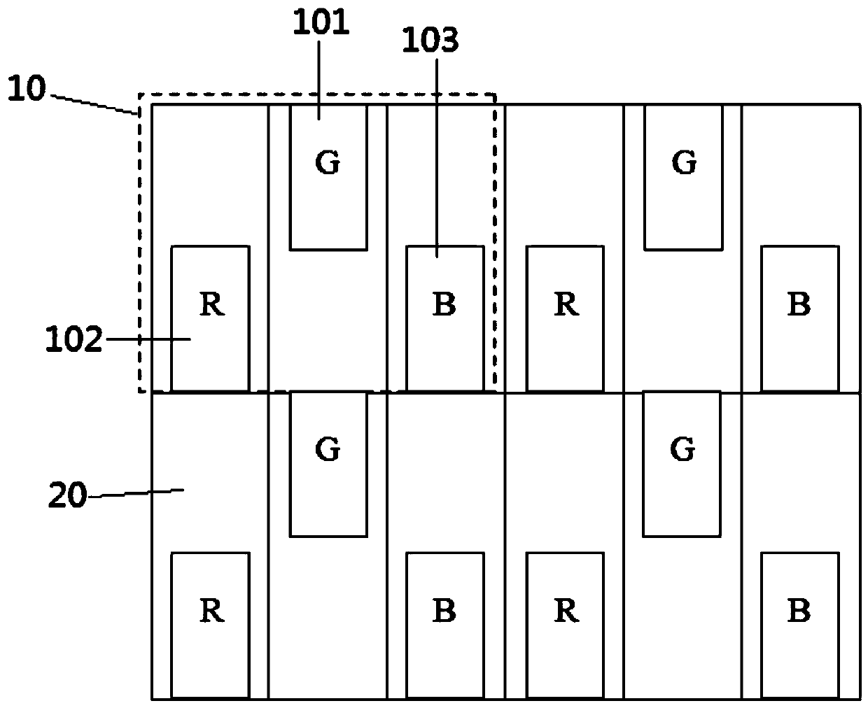
[0042] see Figure 2 ~ Figure 4 , is a schematic diagram of the local layout of the pixel arrangement structure in the first embodiment of the present invention. Such as figure 2 As shown, the pixel structure of the display panel includes: a plurality of pixel groups 10 ; wherein, the pixel group 10 includes a first color pixel 101 , a second color pixel 102 and a third color pixel 103 . Adjacent pixels among the first color pixels 101, the second color pixels 102 and the third color pixels 103 are alternately arranged up and down, that is, adjacent pixels are not on the same straight line, so that the same pixel group 10 The distance between adjacent pixels increases, which improves the LED transfer yield.

[0043] Continue to refer to figure 2 As shown, in the pixel arrangement structure described in this embodiment, several pixel groups 10 are repeatedly arranged along the vertical direction and the horizontal direction. The first color pixel 101 is a red pixel, the s...

no. 2 example

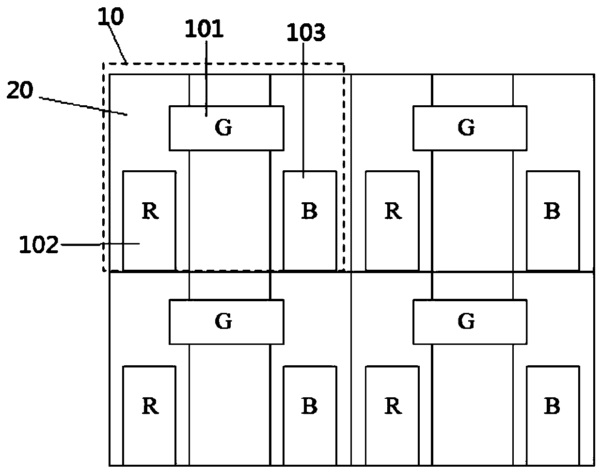
[0050] see Figure 5 ~ Figure 8 , is a schematic diagram of the partial layout of the pixel arrangement structure in the second embodiment of the present invention. The pixel structure of the display panel in this embodiment includes: a plurality of pixel groups 10 ; wherein, the pixel groups 10 include first color pixels 101 , second color pixels 102 and third color pixels 103 . Adjacent pixels among the first color pixels 101, the second color pixels 102 and the third color pixels 103 are alternately arranged up and down, that is, adjacent pixels are not on the same straight line, so that the same pixel group 10 The distance between adjacent pixels increases, which improves the LED transfer yield.

[0051] read on Figure 5 ~ Figure 8 As shown, the pixel group 10 includes a first sub-pixel group 11 and a second sub-pixel group 12 . The first sub-pixel group 11 includes a first color pixel 101 , a second color pixel 102 and a third color pixel 103 . The second sub-pixel g...


PUM


Abstract

The invention provides a pixel arrangement structure, an electroluminescent device and a display device, and the pixel arrangement structure comprises a plurality of pixel groups, each pixel group comprises a plurality of pixels, and the adjacent pixels in each pixel group are arranged in an up-and-down staggered manner. According to the array substrate, the pixels are divided into the plurality of pixel groups, the adjacent pixels in each pixel group are arranged in an up-down staggered manner, and the shapes and the long axis directions of the pixels are changed, so that the distance betweenthe adjacent pixels in a single pixel group is increased; by arranging the sub-pixel groups in mirror symmetry, the pixel distance between the adjacent pixel groups is increased, the LED transfer yield is improved, and the requirements of small-size and high-resolution electroluminescent display devices can be met.

Description

technical field [0001] The invention belongs to the field of display technology, and in particular relates to a pixel arrangement structure, an electroluminescent device and a display device. Background technique [0002] In recent years, electroluminescence (EL) devices have been widely used in the production of display products, such as OLED, mini-LED, micro-LED, etc. Compared with traditional displays such as CRT, LCD, etc., they have better optical characteristics, such as high contrast, High brightness and high color saturation are gradually becoming the mainstream of next-generation displays. [0003] However, the pixel arrangement of existing display products such as mini-LED or micro-LED is as follows: figure 1 The array arrangement is shown, and the distance between adjacent pixels is relatively close. When transferring LEDs, the accuracy of the transfer equipment will be poor, and the pixels transferred later will easily get stuck on the pixels transferred earlier...

Claims


Application Information

Patent Timeline
Patent Type & Authority Applications(China)
IPC IPC(8): H01L27/15
CPCH01L27/15H10K59/352H10K59/353
Inventor 袁山富
Owner CHONGQING KONKA PHOTOELECTRIC TECH RES INST CO LTD
Why Eureka
Try Eureka