Bright and clean x-ray source for x-ray based metrology

一种X射线、光源的技术,应用在巨大电流的X射线管、X射线管、X射线设备等方向,能够解决辐射低能量、限制利用等问题

Active Publication Date: 2020-04-21
KLA CORP
View PDF12 Cites 1 Cited by
  • Summary
  • Abstract
  • Description
  • Claims
  • Application Information

AI Technical Summary

Problems solved by technology

However, the radiation produced is relatively low energy (92.6 electron volts), which severely limits the utilization of these sources of irradiation in metrology applications

Method used


Image

  • Bright and clean x-ray source for x-ray based metrology
  • Bright and clean x-ray source for x-ray based metrology
  • Bright and clean x-ray source for x-ray based metrology

Examples


Embodiment Construction

[0024] Reference will now be made in detail to prior art examples and some embodiments of the invention, examples of which are illustrated in the accompanying drawings.

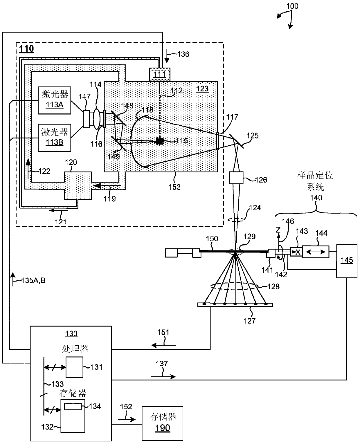
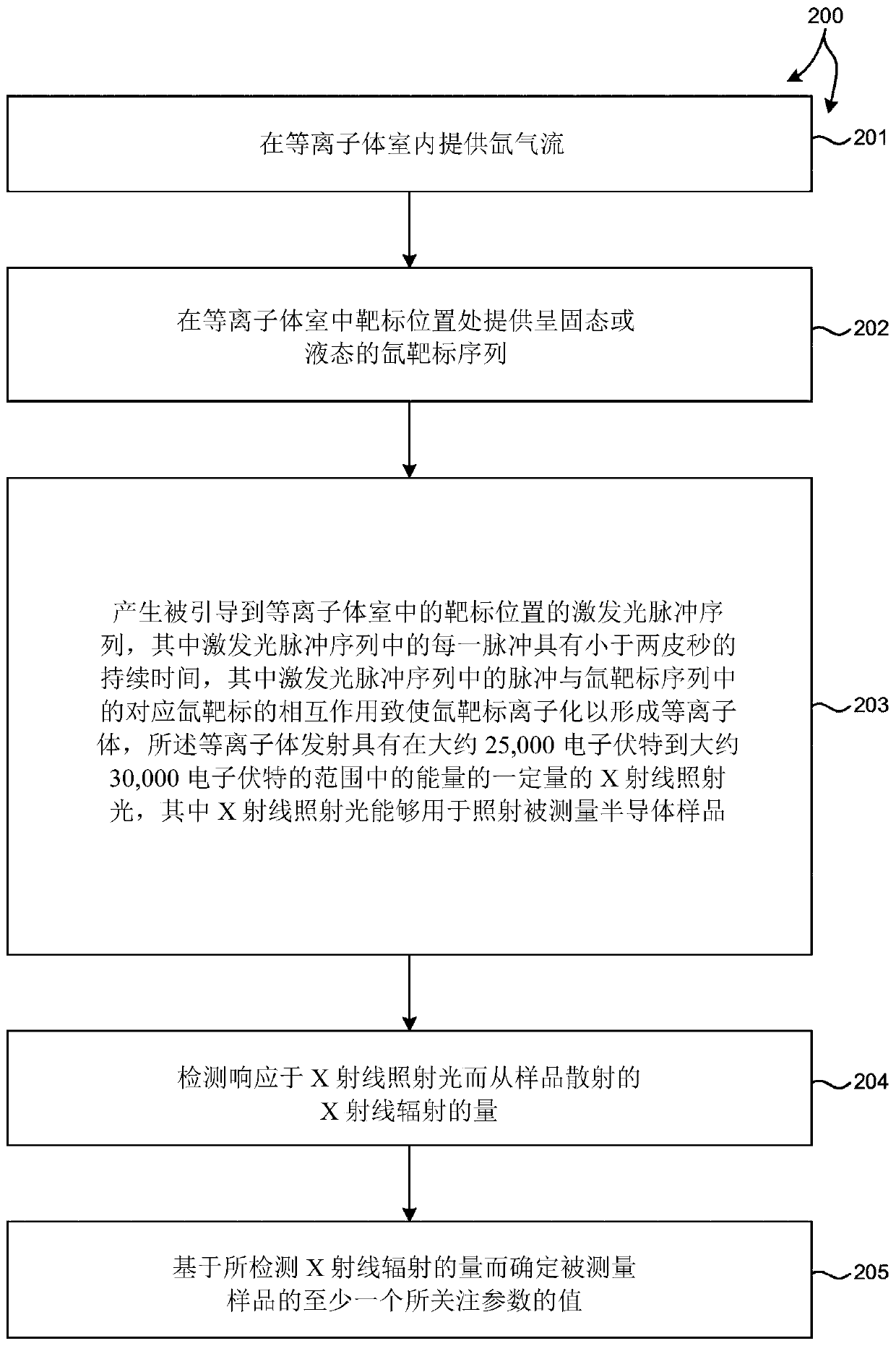
[0025] Methods and systems for x-ray-based semiconductor metrology utilizing clean, rigid x-ray radiation sources are described herein. More specifically, laser-produced plasma (LPP) light sources produce high brightness (that is, greater than 10 13 photon / (second.mm 2 .mrad 2), hard x-ray exposure. To achieve this high brightness, the LPP light source directs a highly focused (e.g., less than 10 micron illumination spot on the target), extremely short duration (e.g., less than 2 picoseconds) laser beam to a dense xenon target in liquid or solid state. The interaction of a focused laser pulse with a high-density xenon target induces a plasma. Radiation from the plasma is collected by collection optics and directed to the sample being measured. Due to the use of non-metallic target materials, the resultin...


PUM

PropertyMeasurementUnit
diameteraaaaaaaaaa

Abstract

Methods and systems for x-ray based semiconductor metrology utilizing a clean, hard X-ray illumination source are described herein. More specifically, a laser produced plasma light source generates high brightness, hard x-ray illumination having energy in a range of 25,000 to 30,000 electron volts. To achieve high brightness, a highly focused, very short duration laser beam is focused onto a denseXenon target in a liquid or solid state. The interaction of the focused laser pulse with the high density Xenon target ignites a plasma. Radiation from the plasma is collected by collection optics and is directed to a specimen under measurement. The resulting plasma emission is relatively clean because of the use of a non-metallic target material. The plasma chamber is filled with Xenon gas to further protect optical elements from contamination. In some embodiments, evaporated Xenon from the plasma chamber is recycled back to the Xenon target generator.

Description

technical field [0001] The described embodiments relate to x-ray laser generated plasma radiation sources and systems for x-ray metrology and inspection. Background technique [0002] Semiconductor devices, such as logic and memory devices, are typically fabricated by a sequence of processing steps applied to a substrate or wafer. Various features and multiple structural levels of the semiconductor device are formed through these processing steps. For example, photolithography, in particular, is a semiconductor fabrication process that involves creating patterns on semiconductor wafers. Additional examples of semiconductor fabrication processes include, but are not limited to, chemical mechanical polishing, etching, deposition, and ion implantation. Multiple semiconductor devices may be fabricated on a single semiconductor wafer and then separated into individual semiconductor devices. [0003] During the semiconductor manufacturing process, metrology processes are used a...

Claims


Application Information

Patent Timeline
Patent Type & Authority Applications(China)
IPC IPC(8): H05G2/00
CPCG01N23/201H05G2/008H05G2/006H05G2/005G01N23/20008
Inventor O·可哈达金
Owner KLA CORP
Why Eureka
Try Eureka