A vacuum high and low temperature semiconductor device test probe station

A test probe, high and low temperature technology, applied in the field of vacuum high and low temperature semiconductor device test probe station, can solve the problems of low replacement efficiency, troublesome replacement, affecting the normal judgment of wafers, etc., and achieve the effect of convenient replacement and convenient use

Active Publication Date: 2020-09-08
合肥芯测半导体有限公司
View PDF6 Cites 0 Cited by
  • Summary
  • Abstract
  • Description
  • Claims
  • Application Information

AI Technical Summary

Problems solved by technology

[0003] The existing vacuum high and low temperature semiconductor device test probe station is cumbersome to replace the probe, and the replacement efficiency is low, and when the probe is used to test the wafer, the surface of the wafer is easily scratched, which further affects the quality of the wafer. The test results cannot be accurate, which affects the normal judgment of the wafer. Therefore, we propose a vacuum high and low temperature semiconductor device test probe station to solve the above problems

Method used


Image

  • A vacuum high and low temperature semiconductor device test probe station
  • A vacuum high and low temperature semiconductor device test probe station
  • A vacuum high and low temperature semiconductor device test probe station

Examples


Embodiment Construction

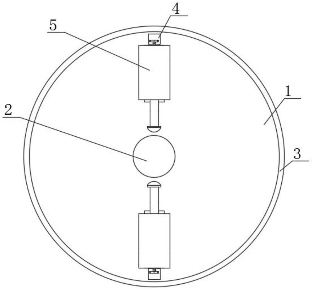
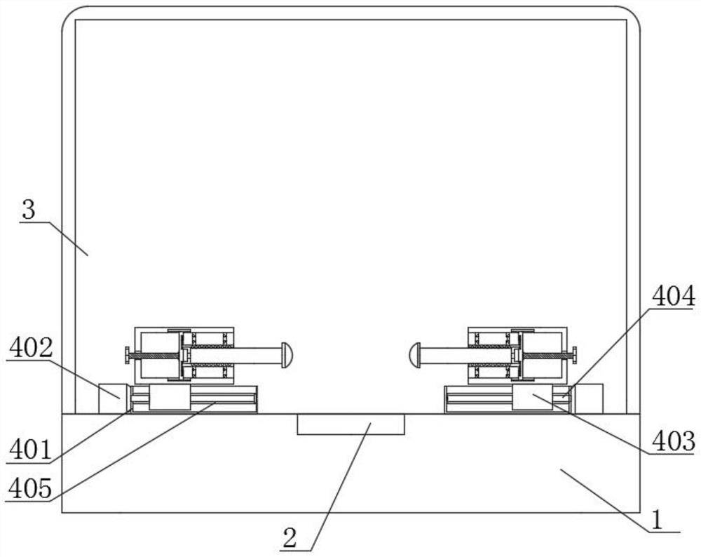
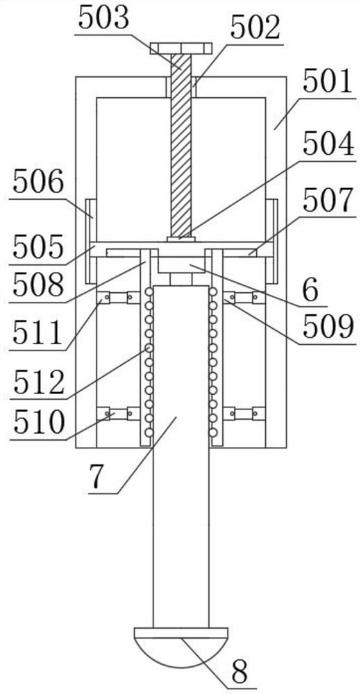
[0023] Such as Figure 1-5 As shown, the embodiment of the present invention provides a vacuum high and low temperature semiconductor device testing probe station, which includes a table body 1, a protective cover 3, a probe rod 7 and a probe head 8. The center of the top surface of the table body 1 is opened There is a placement slot 2, and the workbench body 1 is clamped with the protective cover 3. By setting the placement slot 2, the semiconductor device is placed inside the placement slot 2, so as to facilitate the positioning of the semiconductor device. Both ends of the top surface of the workbench body 1 Both moving mechanisms 4 are fixedly connected with the moving mechanism 4, and the two moving mechanisms 4 both include a moving box 401. The sides of the two moving boxes 401 away from each other are fixedly connected with a micro motor 402. The micro motor 402 of the present invention uses a 5LK60W micro motor. The output ends of the motor 402 are fixedly connected w...


PUM


Abstract

The invention provides a vacuum high-low temperature semiconductor device test probe station, which relates to the technical field of semiconductor devices. The vacuum high-low temperature semiconductor device test probe station comprises a workbench body, a protective cover, a probe rod and a probe head, wherein moving mechanisms are fixedly connected to the two ends of the top surface of the workbench body, each moving mechanism comprises a moving box, and micro motors are fixedly connected to the side surfaces, away from each other, of the two moving boxes. According to the vacuum high-lowtemperature semiconductor device test probe station provided by the invention, as a clamping mechanism is arranged, the advantages of convenience in replacement and use is achieved, and the problems that a probe is troublesome to replace when an existing vacuum high-low temperature semiconductor device test probe station is used for replacing the probe and the replacement efficiency is low can besolved; and as a buffer mechanism is arranged, the conditions that the surface of the wafer is easily stabbed, the testing of the wafer is further influenced, the tested result cannot be accurate andthe normal judgment of the wafer is influenced when the wafer is tested are effectively avoided.

Description

Technical field [0001] The invention relates to the technical field of semiconductor devices, in particular to a vacuum high and low temperature semiconductor device testing probe station. Background technique [0002] Semiconductor devices usually use different semiconductor materials, use different processes and geometric structures, and have developed a wide variety of crystal diodes with different functions and uses. The frequency coverage of crystal diodes can range from low frequency to high frequency. , Microwave, millimeter wave, infrared to light wave, three-terminal devices are generally active devices, and the typical representatives are various transistors (also called transistors). [0003] Existing vacuum high and low temperature semiconductor device testing probe stations are troublesome to replace the probes, and the replacement efficiency is low, and when the probes are testing the wafer, the surface of the wafer is easily damaged, which further affects the wafer. ...

Claims


Application Information

Patent Timeline
Patent Type & Authority Patents(China)
IPC IPC(8): G01R31/26
CPCG01R31/2601
Inventor 刘家铭张孝仁苏华庭
Owner 合肥芯测半导体有限公司
Why Eureka
Try Eureka