Process for solving flatness of display screen module

A display module and flatness technology, applied in the direction of instruments, connecting components, identification devices, etc., can solve the problems that affect the display effect, cannot meet the flatness, and the lamp bead surface of the LED lamp board is prone to warping, etc. Improve flatness and avoid warpage

Active Publication Date: 2020-04-28
LIGHTKING TECH GRP CO LTD
View PDF20 Cites 3 Cited by
  • Summary
  • Abstract
  • Description
  • Claims
  • Application Information

AI Technical Summary

Problems solved by technology

[0004] However, in the existing technology, after GOB packaging, due to the internal stress of the glue, the bead surface of the LED light board is prone to warping, which

Method used


Image

  • Process for solving flatness of display screen module
  • Process for solving flatness of display screen module
  • Process for solving flatness of display screen module

Examples


Example Embodiment

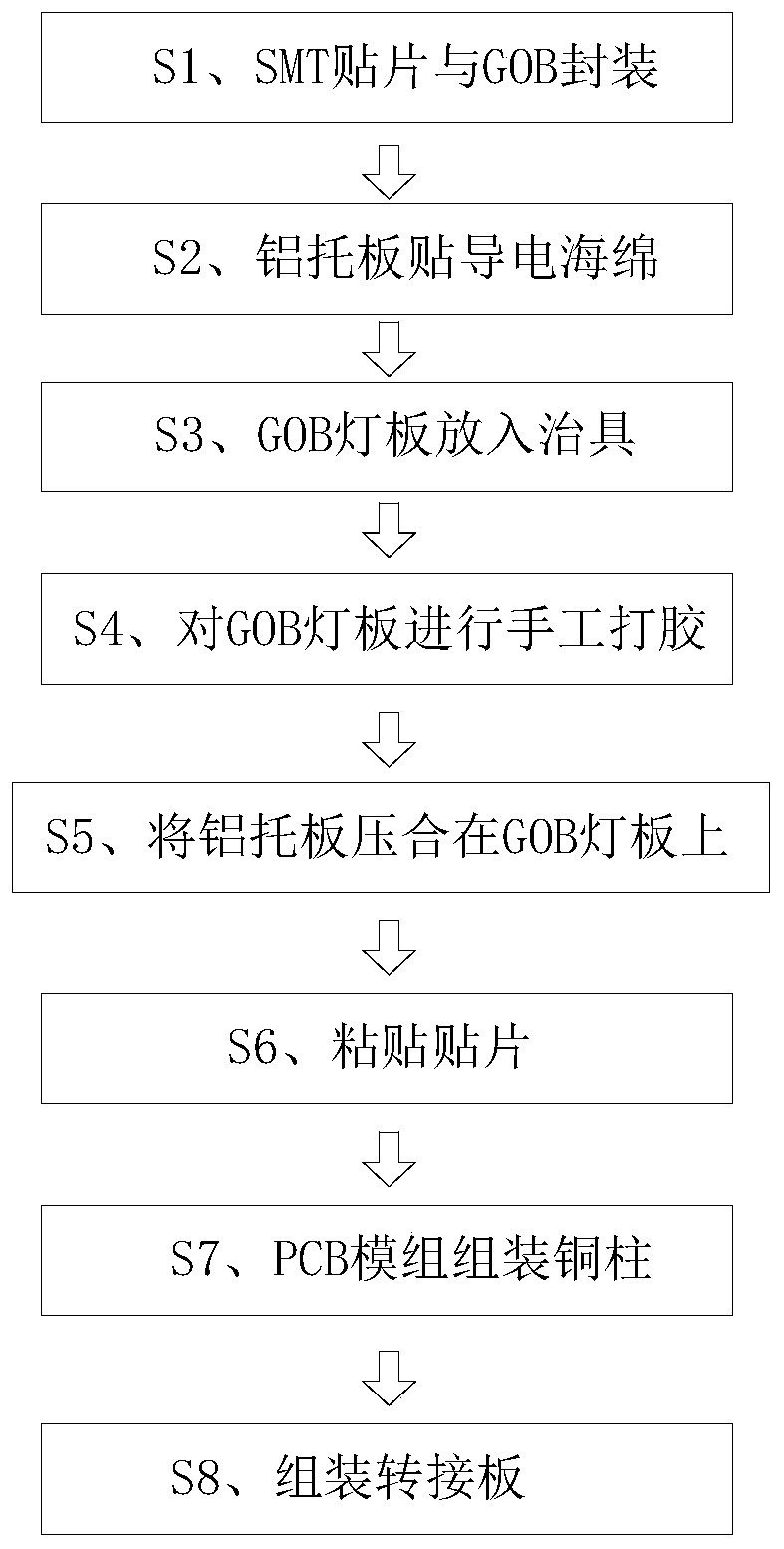
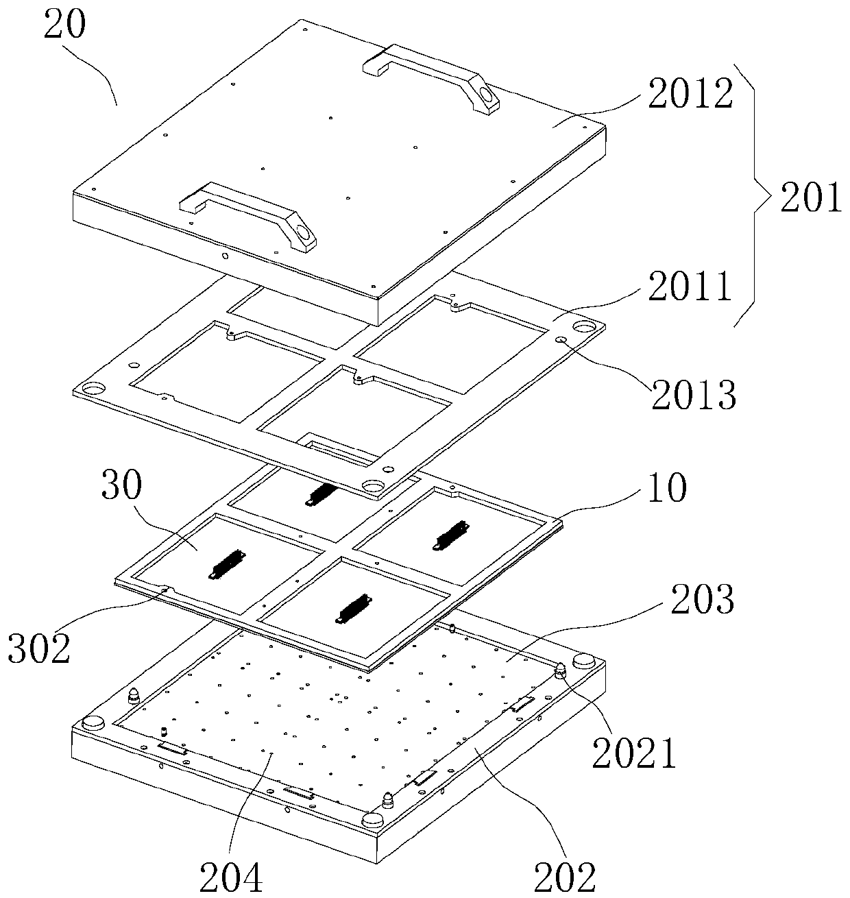
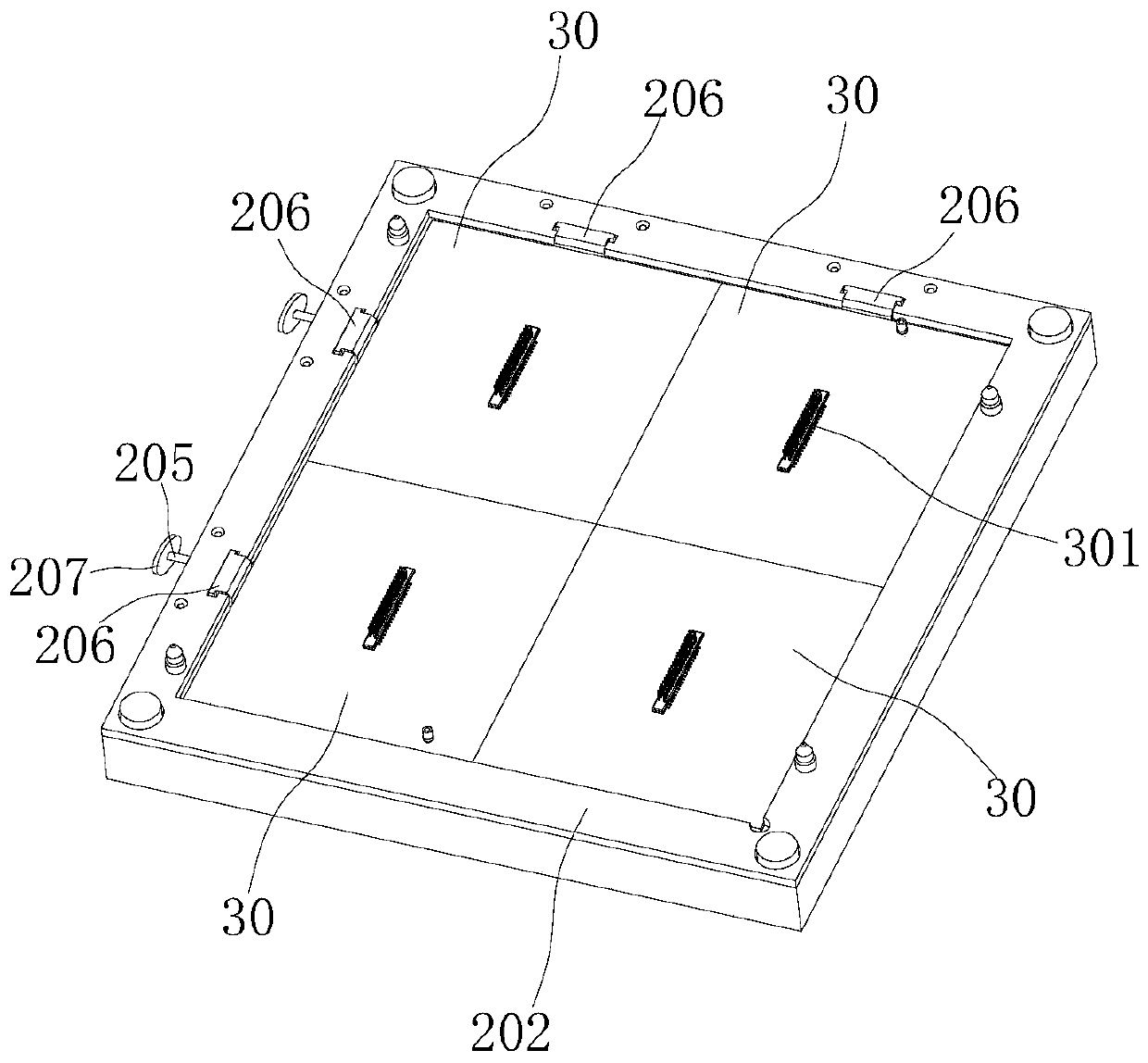
[0032] The present invention will be further described below in conjunction with the drawings and embodiments.

[0033] In the following, the concept, specific structure and technical effects of the present invention will be clearly and completely described in conjunction with the embodiments and the drawings to fully understand the purpose, features and effects of the present invention. Obviously, the described embodiments are only a part of the embodiments of the present invention, rather than all of them. Based on the embodiments of the present invention, other embodiments obtained by those skilled in the art without creative work belong to The scope of protection of the present invention. In addition, all the connection / connection relationships involved in the patent do not only refer to the direct connection of the components, but refer to the fact that a better connection structure can be formed by adding or reducing connection accessories according to specific implementati...


PUM


Abstract

The invention discloses a process for solving the flatness problem of a display screen module, and relates to the technical field of LED display screens. The process comprises the following steps: S1,performing SMT mounting and GOB packaging on a PCB (Printed Circuit Board); S2, attaching conductive sponge to the aluminum supporting plate; S3, placing the PCB lamp panel into a jig; S4, conductinggluing on the PCB lamp panel; S5, pressing the aluminum supporting plate on the PCB lamp panel. The process has the beneficial effects that the warping problem generated after GOB packaging of the LED lamp panels can be effectively avoided, the flatness of the LED lamp panels is greatly improved, and splicing of the multiple LED lamp panels can be achieved.

Description

technical field [0001] The invention relates to the technical field of LED display screens, and more specifically, the invention relates to a process for solving the flatness of the display screen. Background technique [0002] Since the development of the LED display industry, a variety of production and packaging processes have emerged one after another. From the previous in-line (Lamp) process, to the surface mount (SMD) process, to the emergence of COB packaging technology, and finally to the emergence of GOB packaging technology. [0003] SMD: It is the abbreviation of Surface Mounted Devices, which means: surface mount device. The LED products packaged by SMD (Surface Mount Technology) is to package lamp cups, brackets, wafers, leads, epoxy resin and other materials into lamp beads of different specifications. Use a high-speed placement machine to solder the lamp beads on the circuit board with high-temperature reflow soldering to make display units with different pi...

Claims


Application Information

Patent Timeline
IPC IPC(8): G09F9/33F16B11/00
CPCG09F9/33F16B11/00
Inventor 齐泽明何磊戴朝勇
Owner LIGHTKING TECH GRP CO LTD
Why Eureka
Try Eureka