Chip packaging structure and manufacturing method thereof

A technology of chip packaging structure and manufacturing method, applied in semiconductor/solid-state device manufacturing, semiconductor/solid-state device parts, semiconductor devices, etc., can solve problems affecting the quality of semiconductor devices, achieve compact packaging structure and improve product yield , Guarantee the effect of quality

Active Publication Date: 2021-08-03
SHANGHAI XIANFANG SEMICON CO LTD +1
View PDF3 Cites 0 Cited by
  • Summary
  • Abstract
  • Description
  • Claims
  • Application Information

AI Technical Summary

Problems solved by technology

[0004] Therefore, the technical problem to be solved by the present invention is to overcome the defects in the prior art that the packaging structure warps during the multi-chip packaging process and affect the subsequent manufacturing process and the quality of semiconductor devices, thereby providing a new chip packaging structure and its manufacturing method

Method used


Image

  • Chip packaging structure and manufacturing method thereof
  • Chip packaging structure and manufacturing method thereof
  • Chip packaging structure and manufacturing method thereof

Examples


Embodiment approach

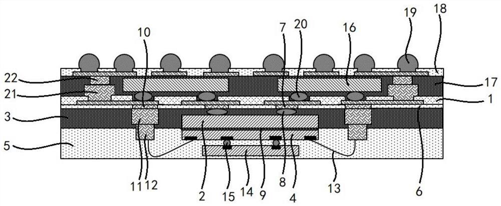
[0105] As an embodiment of the present invention, before making the first plastic package 3, it also includes:

[0106] Making a first conductive column 11 on the dielectric layer 6, the first conductive column 11 is encapsulated by the first plastic package 3;

[0107] After making the first plastic package 3, it also includes:

[0108] A first opening 23 is opened on the first plastic package 3 to expose the end surface of the first conductive column 11 facing away from the dielectric layer 6;

[0109] Make the second conductive post 12 at the first opening 23, so that the second conductive post 12 is electrically connected to the first conductive post 11, and the end face of the second conductive post 12 on the side away from the first conductive post 11 is higher than the first plastic package 3 ;

[0110] Conductive wires 13 are fabricated to connect the second chip 4 and the second conductive pillars 12 .

[0111] The manufacturing method of the chip package structure...


PUM


Abstract

The invention provides a chip packaging structure and a manufacturing method thereof. The chip packaging structure includes: a first rewiring layer; a first chip electrically connected to the first rewiring layer; a first plastic package encapsulating the first chip; a second chip arranged on the first chip away from the first rewiring layer. One side of the wiring layer is electrically connected to the first rewiring layer; the second plastic package encloses the second chip, and the thermal expansion coefficient of the second plastic package is different from that of the first plastic package. The first chip is encapsulated by the first plastic package, and the second chip is packaged by the second plastic package, so that the thermal expansion coefficients of the first plastic package and the second plastic package are different, and the first plastic package and the second plastic package expand during the formation process. Different from the thermal stress caused by shrinkage, it achieves the purpose of balancing the overall stress of the plastic package, thereby reducing the overall warpage of the packaging structure, effectively controlling the warpage during the packaging process, improving the reliability of the package, and facilitating the subsequent semiconductor device manufacturing process. , to ensure the quality of semiconductor devices and improve product yield.

Description

technical field [0001] The invention relates to the technical field of semiconductor packaging, in particular to a chip packaging structure and a manufacturing method thereof. Background technique [0002] With the continuous development of semiconductor technology, three-dimensional stacked semiconductor devices have been widely used as a process that can effectively reduce the physical size of semiconductor devices. In a three-dimensional package-on-package semiconductor device, active circuits such as logic, memory, processor circuits, etc. are fabricated on separate wafers and packages. Two or more packages are mounted one on top of the other, ie stacked, to allow a higher level of integration of the packages. In addition, stack-package semiconductor devices can achieve smaller form factors, higher cost-effectiveness, enhanced performance, and lower power consumption. [0003] In the prior art, the overall plastic packaging or step-by-step plastic packaging is usually ...

Claims


Application Information

Patent Timeline
Patent Type & Authority Patents(China)
IPC IPC(8): H01L23/29H01L23/31H01L21/56
CPCH01L23/293H01L23/3107H01L23/3135H01L21/56H01L2224/16145H01L2224/73265H01L2924/181H01L2224/48091H01L2224/73253H01L2224/16225H01L2924/00012H01L2924/00014
Inventor 张凯耿菲曹立强
Owner SHANGHAI XIANFANG SEMICON CO LTD
Why Eureka
Try Eureka