Semiconductor device and preparation method thereof

A semiconductor and device technology, applied in the field of semiconductor devices and their preparation, can solve problems such as channel lattice defects, affecting the performance and reliability of semiconductor devices, avoid lattice defects, ensure performance and reliability, and have strong applicability Effect

Active Publication Date: 2020-05-08
INST OF MICROELECTRONICS CHINESE ACAD OF SCI
View PDF5 Cites 0 Cited by
  • Summary
  • Abstract
  • Description
  • Claims
  • Application Information

AI Technical Summary

Problems solved by technology

[0004] However, the formation methods of the above two channels are likely to cause lattice defects in the formed channel, which affects the performance and reliability of the final semiconductor device.

Method used


Image

  • Semiconductor device and preparation method thereof
  • Semiconductor device and preparation method thereof
  • Semiconductor device and preparation method thereof

Examples


Embodiment Construction

[0064] The specific implementation manners according to the present invention will be described below in conjunction with the accompanying drawings.

[0065] In the following description, many specific details are set forth in order to fully understand the present invention, but the present invention can also be implemented in other ways different from those described here, therefore, the present invention is not limited to the specific embodiments disclosed below limit.

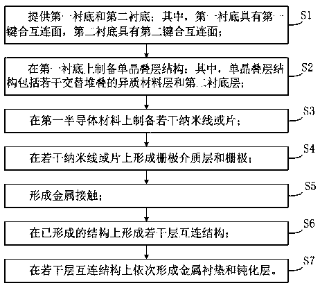
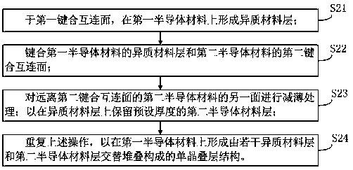
[0066] As the feature size of integrated circuits continues to shrink, especially to nodes below 5nm, traditional tri-gate or double-gate FinFET devices cannot continue to shrink due to their own structural problems. To solve this problem, the GAA structure can be used. Specifically, the GAA structure can adjust the size of stacked nanowires or sheet gate-around devices to ensure that the gate can be on the top and sides of the channel, but also below the channel.

[0067] The channels in the existing stac...


PUM

PropertyMeasurementUnit
Layer thicknessaaaaaaaaaa

Abstract

The invention discloses a preparation method of a semiconductor device. The preparation method comprises the following steps: providing a first substrate and a second substrate, wherein the first substrate is provided with a first bonding interconnection surface, and the second substrate is provided with a second bonding interconnection surface; preparing a single crystal laminated structure on the first substrate, wherein the single crystal laminated structure comprises a plurality of heterogeneous material layers and second substrate layers which are alternately stacked; preparing a plurality of nanowires or sheets on the first substrate; forming a gate dielectric layer and a gate on the plurality of nanowires or sheets; forming a metal contact; forming a plurality of layers of interconnection structures on the formed structure; and sequentially forming a metal liner and a passivation layer on the plurality of layers of interconnection structures. The channel material formed by the preparation method does not have lattice imperfection, can avoid influencing the performance and reliability of a subsequently formed device, and does not limit the forming process of a subsequent structure; and the preparation method has good applicability. The invention also provides a semiconductor device.

Description

technical field [0001] The invention relates to the technical field of semiconductors, in particular to a semiconductor device and a preparation method thereof. Background technique [0002] As the feature size of integrated circuits continues to shrink, especially at nodes below 5nm, traditional triple-gate or double-gate Fin Field-Effect Transistor (Fin Field-Effect Transistor, abbreviated as FinFET) devices cannot continue to shrink due to their own structural problems. To solve this problem, a Gate-All-Around (Gate-All-Around, abbreviated as GAA) structure can be used. The GAA structure can adjust the size of stacked nanowire or sheet gate-around devices to ensure that the gate can be on the top and sides of the channel, but also below the channel. [0003] Channels in existing stacked nanowires or sheet-ring-gate devices are generally formed by epitaxy using an STI first process, or are realized by periodically forming Si / SiGe stacks by using an STI last process. [0...

Claims


Application Information

Patent Timeline
IPC IPC(8): H01L29/06H01L21/336H01L29/78
CPCH01L29/0669H01L29/0673H01L29/66795H01L29/785
Inventor 殷华湘张青竹徐忍忍
Owner INST OF MICROELECTRONICS CHINESE ACAD OF SCI
Why Eureka
Try Eureka