Gallium Oxide Based Heterojunction Semiconductor Structures and Devices

A gallium oxide and heterojunction technology, applied in semiconductor devices, electrical components, circuits, etc., can solve the problems of poor band structure matching, difficult material preparation process, poor crystal structure matching, etc., to improve forward input transport performance, avoid dislocation defects, and improve the effect of current transport capability

Active Publication Date: 2022-05-06
合肥中科微电子创新中心有限公司
View PDF0 Cites 0 Cited by
  • Summary
  • Abstract
  • Description
  • Claims
  • Application Information

AI Technical Summary

Problems solved by technology

[0007] In order to solve the problems of poor band structure matching, poor crystal structure matching, difficult material preparation process, and high preparation cost in the heterogeneous PN junction structure formed by the above-mentioned P-type material and gallium oxide, the present invention proposes a gallium oxide-based Heterojunction semiconductor structures and their devices

Method used


Image

  • Gallium Oxide Based Heterojunction Semiconductor Structures and Devices
  • Gallium Oxide Based Heterojunction Semiconductor Structures and Devices
  • Gallium Oxide Based Heterojunction Semiconductor Structures and Devices

Examples


Embodiment Construction

[0029] In order to make the object, technical solution and advantages of the present invention clearer, the present invention will be described in further detail below in conjunction with specific embodiments and with reference to the accompanying drawings.

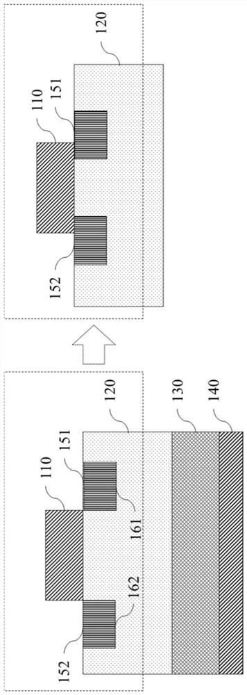
[0030] One aspect of the present invention discloses a heterojunction semiconductor structure based on gallium oxide. The structure includes: at least one gallium oxide base layer with multiple contact surfaces; at least one delafossite layer through multiple contact surfaces. At least one of the contact surfaces or a portion of one of the plurality of contact surfaces forms a heterojunction structure with the gallium oxide-based layer. Here, the gallium oxide base layer can be selected as an n-type gallium oxide base layer. The gallium oxide base layer can be doped or improved in various ways. The improvement is not limited to the improvement of the material composition, but also the improvement of the structure, such as ...


PUM


Abstract

The invention discloses a heterojunction semiconductor structure based on gallium oxide. The structure includes: at least one gallium oxide base layer, the gallium oxide base layer has multiple contact surfaces; The gallium-based layer forms a heterojunction structure. Through this structure, the present invention realizes the matching of the forbidden band width, the matching of the conduction band and the matching of the valence band, and improves the current transport capability of the structure; in addition, the heterogeneous PN junction structure also realizes the matching of the crystal structure, It avoids the formation of a large number of dislocation defects at the contact surface of the heterogeneous PN junction, improves the forward transport performance of the PN junction, the on-resistance of the device using this structure, and the stability of the device performance; finally, the delafossite material The preparation process is simple, and it can be directly formed by a similar sol-gel method or hydrothermal synthesis method, which greatly reduces the preparation cost and process of the structure, and is easy to realize large-scale industrial production.

Description

technical field [0001] The invention relates to the technical field of semiconductors, in particular to a gallium oxide-based heterojunction semiconductor structure and a device thereof. Background technique [0002] Seeking wider band gap and higher material performance is an important trend in the development of compound semiconductor materials. Gallium oxide (Ga 2 o 3 ) semiconductor has a large forbidden band width (E g ~4.8eV), high breakdown field strength (E br ~8MV / cm), Baliga high quality factor (εμE br 3 ~3444), low growth cost (melting method to produce single crystal substrate) and other outstanding advantages, it is used for next-generation high-voltage high-power devices (such as Schottky barrier diodes (SBD), field effect transistors (MOSFET)), power One of the preferred materials for IC circuits and solar-blind ultraviolet photoelectric (200-280nm band) detectors. [0003] High-voltage and high-power devices have significant power conversion and energy...

Claims


Application Information

Patent Timeline
Patent Type & Authority Patents(China)
IPC IPC(8): H01L29/267
CPCH01L29/267
Inventor 龙世兵向学强丁梦璠徐光伟赵晓龙刘明
Owner 合肥中科微电子创新中心有限公司
Why Eureka
Try Eureka