Display substrate, manufacturing method thereof and display device

A technology for displaying substrates and manufacturing methods, which is applied in the fields of mechanically removing conductive materials, manufacturing printed circuits, manufacturing semiconductors/solid-state devices, etc. It can solve problems such as DGS, electrostatic breakdown, and display abnormalities, and improve reliability , to avoid the effect of short circuit

Pending Publication Date: 2020-05-19
HEFEI XINSHENG OPTOELECTRONICS TECH CO LTD +1
3 Cites 2 Cited by

AI-Extracted Technical Summary

Problems solved by technology

[0003] Embodiments of the present invention provide a display substrate, a manufacturing method thereof, and a display device, so as to solve the problem in...

Method used

[0039] In an embodiment of the present invention, the display substrate includes first conductive traces and second conductive traces respectively extending in different directions, the first conductive traces and the second conductive traces intersect in the target area, and the first The surface in contact with the insulating layer in the first part of the conductive trace located in the target area is designed to be parallel to the base substrate, which can avoid the problem of electrostatic breakdown of the tip caused by the tip of the first part, thereby avoiding the first conductive In the event that the wiring and the second conductive wiring are short-circuited at the intersection position, the reliability of the display device is improved. Therefore, the technical solution provided by the present invention can improve the reliability of the display device.
[0043] Because the target portion 121 of the first conductive trace 120 is parallel to the base substrate 110 near the second conductive trace 130, the target portion 131 of the second conductive trace 130 is close to the first conductive trace 120. Parallel to the base substrate 110, so that the distance between the first part 121 and the target part 131 is equal, and the problem of electrostatic breakdown of the tip will not be caused, thereby preventing the crossing position of the first conductive trace 120 and the second conductive trace 130 A short circuit occurs between them, improving the reliability of the display device.
[0053] The support pattern 160 is connected to the first conductive trace 120, and can also be used to transmit signals on the first conductive trace 120 as a conductive pattern, which considerably increases the thickness of the first conductive trace 120 in the groove 151 , the resistivity of signal transmission is reduced, ensuring that the signal on the first conductive trace 120 can be normally trans...

Abstract

The invention provides a display substrate, a manufacturing method thereof and a display device. The display substrate comprises a first conductive wire, a second conductive wire and an insulating layer, wherein the first conductive wire is located on a substrate and extends in a first direction, the second conductive wire extends in a second direction, and the insulating layer is located betweenthe first conductive wire and the second conductive wire. The display substrate further comprises a buffer layer located on the side, close to the substrate, of the insulating layer, a groove extending in the first extending direction is formed in the buffer layer, and the surface of the side, away from the substrate, of the first conductive wire is flush with the surface of the side, away from the substrate, of the buffer layer. According to the display substrate, the manufacturing method thereof and the display device, the reliability of the display device can be improved.

Application Domain

Technology Topic

Image

  • Display substrate, manufacturing method thereof and display device
  • Display substrate, manufacturing method thereof and display device
  • Display substrate, manufacturing method thereof and display device

Examples

  • Experimental program(1)

Example Embodiment

[0037] The following will clearly and completely describe the technical solutions in the embodiments of the present invention with reference to the accompanying drawings in the embodiments of the present invention. Obviously, the described embodiments are some of the embodiments of the present invention, but not all of them. Based on the embodiments of the present invention, all other embodiments obtained by persons of ordinary skill in the art without creative efforts fall within the protection scope of the present invention.
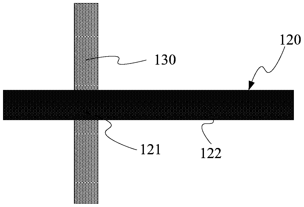
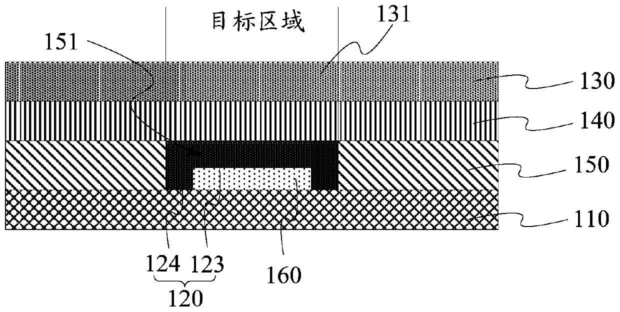
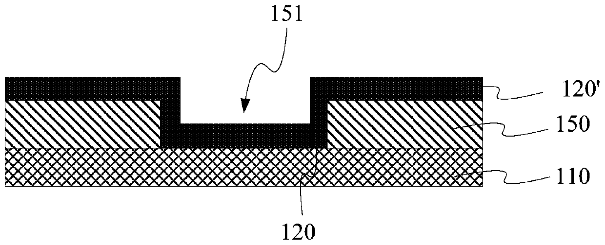
[0038] An embodiment of the present invention provides a display substrate, such as figure 1 and figure 2 As shown, it includes a first conductive trace 120 extending along a first direction on the base substrate 110, a second conductive trace 130 extending along a second direction, and a first conductive trace 120 and a second conductive trace 130. The insulating layer 140 between the two conductive traces 130; the first conductive trace 120 and the second conductive trace 130 intersect in the target area; wherein, the first conductive trace 120 includes a The inner first part 121 and the second part 122 other than the first part 121, the surface of the first part 121 in contact with the insulating layer is parallel to the base substrate.
[0039] In the embodiment of the present invention, the display substrate includes first conductive traces and second conductive traces respectively extending in different directions. The first conductive traces and the second conductive traces intersect in the target area. The surface in contact with the insulating layer in the first part located in the target area is designed to be parallel to the base substrate, which can avoid the problem of electrostatic breakdown of the tip caused by the tip of the first part, thereby avoiding the first conductive trace and When the second conductive wires are short-circuited at the intersection position, the reliability of the display device is improved. Therefore, the technical solution provided by the present invention can improve the reliability of the display device.
[0040] The above display substrate may be a flexible display substrate or a rigid display substrate. When the display substrate is a flexible display substrate, the substrate substrate 110 adopts a flexible substrate substrate, such as a polyimide film; when the display substrate is a rigid display substrate, the substrate substrate 110 adopts a rigid substrate substrate, such as a quartz substrate or a glass substrate. substrate.
[0041] The above-mentioned first conductive traces 120 and second conductive traces 130 may be two conductive traces that extend in different directions in the display substrate and are adjacent in layer distribution, for example, they are connected to the same thin film transistor (Thin Film Transistor, TFT for short). grid lines and data lines.
[0042] like figure 1 As shown, the first conductive trace 120 includes a first portion 121 located in the target area and a second portion 122 other than the first portion 121, wherein, as figure 2 As shown, the contact surface between the first part 121 and the insulating layer 140 is parallel to the base substrate 110, so that the insulating layer 140 has a flat structure in the target area, that is, the insulating layer 140 in the target area is close to the side surface of the base substrate 110 It is parallel to the base substrate 110 , and the surface of the insulating layer 140 in the target region away from the base substrate 110 is parallel to the base substrate 110 . In this way, the surface of the target portion 131 of the second conductive trace 140 formed on the insulating layer 140 and located in the target region near the first conductive trace 120 is parallel to the base substrate 110 .
[0043]Because, the target portion 121 of the first conductive trace 120 is parallel to the substrate 110 near the second conductive trace 130, and the target portion 131 of the second conductive trace 130 is parallel to the substrate 120. The base substrate 110, so that the distance between the first part 121 and the target part 131 is equal, and the problem of electrostatic breakdown of the tip will not be caused, thereby preventing occurrence of short circuit, improving the reliability of the display device.
[0044] Further, it also includes a buffer layer 150 located on the side of the insulating layer 140 close to the base substrate 110, the buffer layer 150 is provided with a groove 151 extending along the first extending direction, and the first conductive The surface of the trace 110 away from the base substrate 110 is flush with the surface of the buffer layer 150 away from the base substrate 110 .
[0045] In this embodiment, the first conductive wire 110 is accommodated in the groove 151 , and the two walls of the groove 151 opposite to each other may be parallel to each other, or may be inclined to each other, which is not limited here. In addition, the height of the first conductive trace 110 in the direction perpendicular to the base substrate 110 is equal to or smaller than the height of the buffer layer 150 in the direction perpendicular to the base substrate 110 .
[0046] In this embodiment, after opening the groove 151 on the buffer layer 150, the first conductive wiring 110 is accommodated in the groove 151, and the first conductive wiring 110 is kept away from the side of the base substrate 110 The surface is flush with the surface of the buffer layer 150 away from the base substrate 110 , so that the surface of the first conductive wiring 110 contacting the insulating layer 140 is parallel to the base substrate 110 .
[0047] It should be noted that the groove 151 may be inside the buffer layer 150, that is, the height of the groove 151 perpendicular to the direction of the base substrate 110 is smaller than the height of the buffer layer 150 perpendicular to the direction of the base substrate 110; The buffer layer 150 is formed, that is, the groove wall of the groove 151 is the buffer layer 150 , and the groove bottom of the groove 151 is the film layer of the buffer layer 150 near the base substrate 110 .
[0048] Further, as figure 2 As shown, the groove 151 also includes a support pattern 160 located on the side of the first conductive trace 120 facing the base substrate 110, and the first conductive trace 120 includes a third part 123 and a fourth part 124, the surface of the third part 123 away from the base substrate 110 is flush with the surface of the fourth part 124 away from the base substrate, and the third part 123 is on the base substrate The orthographic projection on 110 coincides with the orthographic projection of the support pattern 160 on the base substrate 110 .
[0049] In this embodiment, before the support pattern 160 is formed on the first conductive trace 120, a part of the space in the groove 151 is pre-occupied, and a second layer covering the buffer layer 150 is formed during the formation of the first conductive trace 120. When a conductive material layer 120' is used, it is avoided that the volume of the first conductive material layer 120' entering the groove 151 is too large, causing the part of the first conductive material layer 120' corresponding to the groove 151 to be far away from the surface of the substrate on the side of the substrate. The distance of the base substrate 110 is less than the distance of the buffer layer 150 away from the surface of the base substrate from the base substrate 110, such as image 3 shown.
[0050] By adding the support pattern 160, the distance between the part of the first conductive material layer 120' corresponding to the groove 151 away from the surface on the side of the base substrate from the base substrate 110 is greater than the distance from the surface of the buffer layer 150 away from the side of the base substrate. The distance between the substrate substrate 110, such as Figure 4 shown. Subsequent etching can remove the first conductive material layer outside the groove 151, so that the surface of the first conductive trace 110 away from the base substrate 110 and the buffer layer 150 away from the base substrate 110 one side is flush with the surface.
[0051] Wherein, the support pattern 160 can be located in the central position of the groove, such as figure 2 As shown, that is, the fourth part 124 is located on both sides of the third part 123 parallel to the direction of the substrate; it can also be attached to the side wall of the groove, that is, the fourth part 124 is located on the third part 123 and is parallel to the substrate. One side of the substrate direction.
[0052] Further, the support pattern 160 is a conductive pattern.
[0053] The support pattern 160 is connected to the first conductive trace 120, and can also be used to transmit the signal on the first conductive trace 120 as a conductive pattern, which considerably increases the thickness of the first conductive trace 120 in the groove 151 and reduces the The resistivity of signal transmission ensures that the signal on the first conductive trace 120 can be transmitted normally.
[0054] The embodiment of the present invention also provides a method for manufacturing a display substrate, such as Figure 5 As shown, the method includes:
[0055] Step 510: providing a substrate substrate;
[0056] Step 520: forming a first conductive trace extending along a first direction on the base substrate;
[0057] Step 530: Form an insulating layer covering the first conductive wiring on the base substrate, the first conductive wiring includes a first part located in the target area and a first part other than the first part. Two parts, the surface of the first part in contact with the insulating layer is parallel to the base substrate;
[0058] Step 540 : forming a second conductive trace extending along a second direction on the insulating layer, the second conductive trace crossing the first conductive trace within the target area.
[0059] In the embodiment of the present invention, the display substrate includes first conductive traces and second conductive traces respectively extending in different directions. The first conductive traces and the second conductive traces intersect in the target area. The surface in contact with the insulating layer in the first part located in the target area is designed to be parallel to the base substrate, which can avoid the problem of electrostatic breakdown of the tip caused by the tip of the first part, thereby avoiding the first conductive trace and When the second conductive wires are short-circuited at the intersection position, the reliability of the display device is improved. Therefore, the technical solution provided by the present invention can improve the reliability of the display device.
[0060] like figure 1 As shown, the above display substrate may be a flexible display substrate or a rigid display substrate. When the display substrate is a flexible display substrate, the substrate substrate 110 adopts a flexible substrate substrate, such as a polyimide film; when the display substrate is a rigid display substrate, the substrate substrate 110 adopts a rigid substrate substrate, such as a quartz substrate or a glass substrate. substrate.
[0061] The above-mentioned first conductive traces 120 and second conductive traces 130 may be two conductive traces that extend in different directions in the display substrate and are adjacent in layer distribution, for example, they are connected to the same thin film transistor (Thin Film Transistor, TFT for short). grid lines and data lines.
[0062] like figure 1 As shown, the first conductive trace 120 includes a first portion 121 located in the target area and a second portion 122 other than the first portion 121, wherein, as figure 2 As shown, the contact surface between the first part 121 and the insulating layer 140 is parallel to the base substrate 110, so that the insulating layer 140 has a flat structure in the target area, that is, the insulating layer 140 in the target area is close to the side surface of the base substrate 110 It is parallel to the base substrate 110 , and the surface of the insulating layer 140 in the target region away from the base substrate 110 is parallel to the base substrate 110 . In this way, the surface of the target portion 131 of the second conductive trace 140 formed on the insulating layer 140 and located in the target region near the first conductive trace 120 is parallel to the base substrate 110 .
[0063] Because, the target portion 121 of the first conductive trace 120 is parallel to the substrate 110 near the second conductive trace 130, and the target portion 131 of the second conductive trace 130 is parallel to the substrate 120. The base substrate 110, so that the distance between the first part 121 and the target part 131 is equal, and the problem of electrostatic breakdown of the tip will not be caused, thereby preventing occurrence of short circuit, improving the reliability of the display device.
[0064] Further, before the step of forming a first conductive trace extending along a first direction on the base substrate, the method further includes:
[0065] forming a buffer material layer on the base substrate;
[0066] Etching the buffer material layer to form a buffer layer, the buffer layer including grooves extending along the first direction;
[0067] The step of forming a first conductive trace extending along a first direction on the base substrate includes:
[0068] A first conductive trace is formed in the groove, and the surface of the first conductive trace on a side away from the base substrate is flush with the surface of the buffer layer on a side away from the base substrate.
[0069] In this embodiment, after the buffer material layer 150' is formed on the base substrate, as Figure 6a As shown; a mask plate can be used to expose the buffer material layer 150', and after development, a buffer layer 150 including grooves 151 extending along the first direction is obtained, as Figure 6b shown.
[0070] Subsequent by forming the first conductive material layer 120' covering the buffer layer 150, such as Figure 6c As shown; the first conductive material layer 120' outside the groove 151 is etched away, so that the surface on the side away from the base substrate 110 is flush with the surface on the side of the buffer layer 150 away from the base substrate 110 The first conductive trace 120, as Figure 6d shown.
[0071] like figure 2 As shown, in this embodiment, the first conductive traces 110 are accommodated in the groove 151 , and the two walls of the groove 151 opposite to each other can be parallel to each other, or can be inclined to each other, which is not limited here. In addition, the height of the first conductive trace 110 in the direction perpendicular to the base substrate 110 is equal to or smaller than the height of the buffer layer 150 in the direction perpendicular to the base substrate 110 .
[0072] In this embodiment, after opening the groove 151 on the buffer layer 150, the first conductive wiring 110 is accommodated in the groove 151, and the first conductive wiring 110 is kept away from the side of the base substrate 110 The surface is flush with the surface of the buffer layer 150 away from the base substrate 110 , so that the surface of the first conductive wiring 110 contacting the insulating layer 140 is parallel to the base substrate 110 .
[0073] It should be noted that the groove 151 may be inside the buffer layer 150, that is, the height of the groove 151 perpendicular to the direction of the base substrate 110 is smaller than the height of the buffer layer 150 perpendicular to the direction of the base substrate 110; The buffer layer 150 is formed, that is, the groove wall of the groove 151 is the buffer layer 150, and the groove bottom of the groove 151 is the film layer of the buffer layer 150 on the side close to the base substrate 110
[0074] Further, before the step of forming the buffer material layer on the base substrate, it also includes:
[0075] forming a support material layer on the base substrate;
[0076] Etching the support material layer to form a support pattern, the orthographic projection of the support pattern on the base substrate is located within the orthographic projection of the groove on the base substrate.
[0077]In this embodiment, after forming the supporting material layer 160' on the base substrate, as Figure 7a As shown; the mask plate can be used to expose the support material layer 160', and after development, the support pattern 160 is obtained, such as Figure 7b shown.
[0078] In this embodiment, before the support pattern 160 is formed on the first conductive trace 120, a part of the space in the groove 151 is pre-occupied, and a second layer covering the buffer layer 150 is formed during the formation of the first conductive trace 120. When a conductive material layer 120' is used, it is avoided that the volume of the first conductive material layer 120' entering the groove 151 is too large, causing the part of the first conductive material layer 120' corresponding to the groove 151 to be far away from the surface of the substrate on the side of the substrate. The distance of the base substrate 110 is less than the distance of the buffer layer 150 away from the surface of the base substrate from the base substrate 110, such as image 3 shown.
[0079] By adding the support pattern 160, the distance between the part of the first conductive material layer 120' corresponding to the groove 151 away from the surface on the side of the base substrate from the base substrate 110 is greater than the distance from the surface of the buffer layer 150 away from the side of the base substrate. The distance between the substrate substrate 110, such as Figure 4 shown. Subsequent etching can remove the first conductive material layer outside the groove 151, so that the surface of the first conductive trace 110 away from the base substrate 110 and the buffer layer 150 away from the base substrate 110 one side is flush with the surface.
[0080] Further, the support pattern 160 is a conductive pattern.
[0081] The support pattern 160 is connected to the first conductive trace 120, and can also be used to transmit the signal on the first conductive trace 120 as a conductive pattern, which considerably increases the thickness of the first conductive trace 120 in the groove 151 and reduces the The resistivity of signal transmission ensures that the signal on the first conductive trace 120 can be transmitted normally.
[0082] Further, the step of forming a first conductive trace extending along a first direction on the base substrate includes:
[0083] forming a first conductive material layer covering the groove on the base substrate;
[0084] Etching the first conductive material layer to form a first conductive trace, the first conductive trace includes a third part and a fourth part, the third part is away from the surface on the side of the base substrate and the The surface of the fourth part away from the base substrate is flush, and the orthographic projection of the third part on the base substrate coincides with the orthographic projection of the supporting figure on the base substrate.
[0085] exist Figure 7b on the basis of Figure 6a and Figure 6b The manner shown can be fabricated to form the structure of the buffer layer 150, such as Figure 7c shown.
[0086] through the Figure 7c A first conductive material layer 120' covering the groove is formed on the shown structure, as Figure 7d shown; etching the first conductive material layer 120' to form the first conductive wiring 120, as Figure 7e shown.
[0087] Wherein, the support pattern 160 can be located in the central position of the groove, such as figure 2 As shown, that is, the fourth part 124 is located on both sides of the third part 123 parallel to the direction of the substrate; it can also be attached to the side wall of the groove, that is, the fourth part 124 is located on the third part 123 and is parallel to the substrate. One side of the substrate direction.
[0088] follow-up based on Figure 7e The structure forming the insulating layer 140 is as Figure 7f As shown, the structure for further forming the second conductive wiring 130 is as Figure 7g shown.
[0089] in, Figure 7d to Figure 7e In the process, the step of etching the first conductive material layer to form the first conductive wiring includes:
[0090] The first conductive material layer is etched by using a half-tone mask to remove a portion of the first conductive material layer on a side of the buffer layer away from the base substrate.
[0091] because Figure 7d The required etching depth of the first conductive material layer 120' in the target area is greater than the required etching depth of other areas, and the half-tone mask can be used to achieve different etching depths for the first conductive material layer 120' in different areas. , so that the final etch is obtained as Figure 7e The first conductive trace 120 in which the surface on the side away from the base substrate 110 is flush with the surface of the buffer layer 150 on the side away from the base substrate 110 .
[0092] An embodiment of the present invention also provides a display device, including the above-mentioned display substrate.
[0093] The display device may be a monitor, a mobile phone, a tablet computer, a television, a wearable electronic device, a navigation display device, and the like.
[0094] Unless otherwise defined, the technical terms or scientific terms used in the present disclosure shall have the usual meanings understood by those skilled in the art to which the present invention belongs. "First", "second" and similar words used in the present disclosure do not indicate any order, quantity or importance, but are only used to distinguish different components. "Comprising" or "comprising" and similar words mean that the elements or items appearing before the word include the elements or items listed after the word and their equivalents, without excluding other elements or items. Words such as "connected" or "connected" are not limited to physical or mechanical connections, but may include electrical connections, whether direct or indirect. "Up", "Down", "Left", "Right" and so on are only used to indicate the relative positional relationship. When the absolute position of the described object changes, the relative positional relationship may also change accordingly.
[0095] It will be understood that when an element such as a layer, film, region, or substrate is referred to as being "on" or "under" another element, it can be "directly on" or "under" the other element, Or intervening elements may be present.
[0096] Embodiments of the present invention have been described above in conjunction with the accompanying drawings, but the present invention is not limited to the above-mentioned specific implementations, and the above-mentioned specific implementations are only illustrative, rather than restrictive, and those of ordinary skill in the art will Under the enlightenment of the present invention, without departing from the gist of the present invention and the protection scope of the claims, many forms can also be made, all of which belong to the protection of the present invention.

PUM

no PUM

Description & Claims & Application Information

We can also present the details of the Description, Claims and Application information to help users get a comprehensive understanding of the technical details of the patent, such as background art, summary of invention, brief description of drawings, description of embodiments, and other original content. On the other hand, users can also determine the specific scope of protection of the technology through the list of claims; as well as understand the changes in the life cycle of the technology with the presentation of the patent timeline. Login to view more.

Similar technology patents

Power distribution network electrical equipment monitoring system

InactiveCN108508307AAvoid short circuitImprove securityTesting using acoustic measurementsTesting using optic methodsEmbedded systemCollections data
Owner:LANGFANG POWER SUPPLY COMPANY STATE GRID JIBEI ELECTRIC POWER COMPANY +1

Classification and recommendation of technical efficacy words

  • Avoid short circuit
  • Improve reliability

Arc-shaped cutting anastomat

ActiveCN101912284AGood assembly firmnessImprove reliabilitySurgical staplesDistal anastomosisEngineering
Owner:CHANGZHOU JIANRUIBAO MEDICAL DEVICES

Distributed power harvesting systems using DC power sources

ActiveUS20080143188A1Improve reliabilitySafe operating voltageDc network circuit arrangementsBatteries circuit arrangementsTransverterVoltage variation
Owner:SOLAREDGE TECH LTD
Why Eureka
Try Eureka