
Novel super-barrier power device and manufacturing method thereof

A technology of a power device and a manufacturing method, which is applied to a new type of super-barrier power device and its manufacturing field, can solve the problems of small reverse recovery peak current, short reverse recovery time, and high reverse blocking voltage, and achieve reverse recovery. Small peak current, short reverse recovery time, and lower on-voltage drop

Pending Publication Date: 2020-05-22
FOUNDER MICROELECTRONICS INT
View PDF6 Cites 0 Cited by
  • Summary
  • Abstract
  • Description
  • Claims
  • Application Information

AI Technical Summary

Problems solved by technology

[0006] The purpose of the present invention is to provide a new type of manufacturing method for super-barrier power devices, aiming to solve the problem that existing power devices

Method used


Image

  • Novel super-barrier power device and manufacturing method thereof
  • Novel super-barrier power device and manufacturing method thereof
  • Novel super-barrier power device and manufacturing method thereof

Examples


Embodiment 1

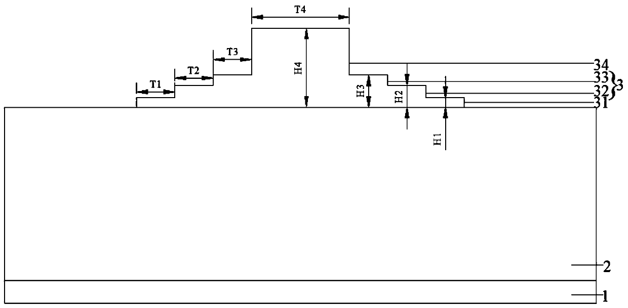
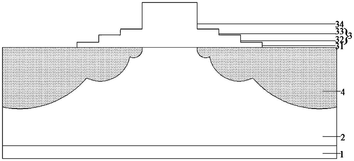
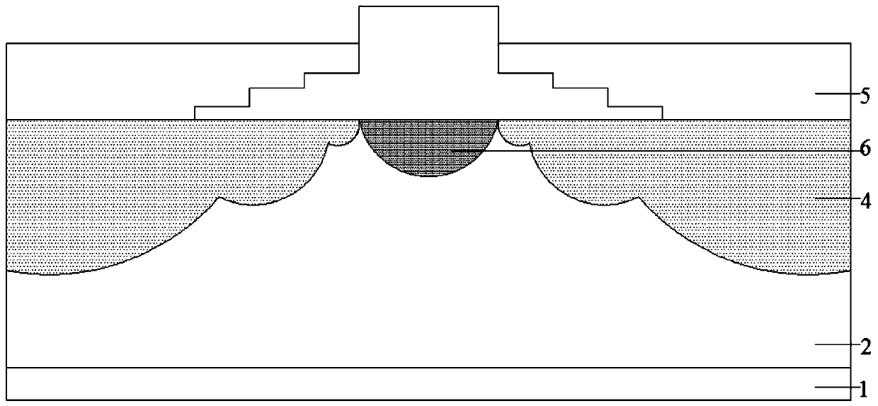
[0066] see Figure 1-7 , this implementation 1 provides a method for manufacturing a novel super-barrier power device, which specifically includes the following steps:

[0067] (1). Provide an N-type substrate including an N-type epitaxial layer; the resistivity of the N-type substrate is <0.005Ω / cm, the thickness of the N-type epitaxial layer is 9 μm, and the resistivity is 2.5Ω / cm, the figure is omitted;

[0068] (2). On the N-type epitaxial layer 2, grow a silicon oxide layer with a thickness of 7500 angstroms at 1050 ° C, and form a ladder structure after three photolithography and etching, that is, the first oxide layer 31, the second oxide layer 32, the third oxide layer Oxide layer 33, specifically as figure 1 As shown, among them, T1>2T2=2T3=2T4, H4>2H3, H3>H2>H1, T1 is 2μm, see details figure 1 .

[0069] (3). Perform P-type ion implantation on the surface of N-type epitaxial layer 2, implantation energy 110KeV, implantation dose 3E13; the implantation energy for P...


PUM

PropertyMeasurementUnit
Widthaaaaaaaaaa

Abstract

The invention provides a novel super-barrier power device and a manufacturing method thereof. The manufacturing method comprises the following steps: forming an oxide layer with a stepped structure onthe surface of an N-type epitaxial layer of an N-type substrate, forming a first P-type injection region and a first N-type injection region on the surface of the N-type epitaxial layer, forming a second P-type injection region in the first N-type injection region, and forming a second N-type injection region in the first P-type injection region; forming a polycrystalline silicon layer on the surface of the oxide layer; and depositing front and back metal layers. The comprehensive device performance of the novel super-barrier power device obtained by adopting the manufacturing method is superior to that of a device chip with a traditional structure, and the leakage current level is far lower than that of a traditional device.

Description

technical field [0001] The invention belongs to the technical field of power devices, and in particular relates to a novel super-barrier power device and a manufacturing method thereof. Background technique [0002] The power device chip is a key component of the circuit system, widely used in high-frequency inverters, digital products, generators, televisions and other civilian products and satellite receivers, missiles and aircraft and other advanced weapon control systems and instrumentation equipment Military occasions. Power device chips are expanding in two important directions: [0003] (1) Developing to tens of millions or even tens of thousands of amperes, it can be mainly used in high temperature arc wind tunnels, resistance welding machines and other occasions; [0004] (2) The reverse recovery time is getting shorter and shorter, and it is developing in the direction of ultra-fast, ultra-soft, and ultra-durable, so that it can not only be used in rectification ...

Claims


Application Information

Patent Timeline
IPC IPC(8): H01L29/06H01L21/8222
CPCH01L29/0634H01L21/8222H01L29/0615Y02P70/50
Inventor 李明刘国梁赵圣哲李理
Owner FOUNDER MICROELECTRONICS INT
Learn More