Ultralow-loss low-end ideal diode

An ideal diode, ultra-low technology, used in data processing power supply, electrical digital data processing, digital data processing components and other directions, can solve the problems of large on-resistance, large current loss, high cost, simple circuit, prevent backflow , cheap effect

Pending Publication Date: 2020-05-22
GUANGZHOU AOGE INTELLIGENT TECH CO LTD
View PDF1 Cites 2 Cited by
  • Summary
  • Abstract
  • Description
  • Claims
  • Application Information

AI Technical Summary

Problems solved by technology

Using a diode in series with the power supply, the circuit is simple, the defect is that the diode has a voltage drop of about 0.6V, and the voltage drop will be proportional to the power loss of the input current
As the current increases, the voltage drop will also increase. For example, replacing it with a Schottky diode can reduce the power, but the power loss is relatively large: Take the Schottky diode SS54 as an example, the corresponding currents of 0.1A, 1A, 10A, and 20A The voltage drops are 0.3V, 0.4V, 0.85V, and 1.4V, and the corresponding losses are 0.03W, 0.4W, 8.5W, and 28W, which means that the greater the passing current, the greater the loss
The disadvantage of Schottky diodes is the voltage drop, which is converted to current loss, and its quiescent current loss is at least milliampere level
[0006] MCU+PMOS tube solution: circuit characteristics require an additional auxiliary voltage, microcontroller (MCU), use MCU's two-way AD to collect voltage on the drain (D pole) and source (S pole) of the PMOS tube, compare The voltage of the two controls the turn-on and cut-off of the PMOS transistor. The disadvantage is that the working current consumption is at least milliampere level, the current loss is very large, and additional auxiliary voltage and MCU are required, and the cost of the solution is high.
[0007] NPN pair tube + NMOS tube scheme: the circuit characteristics require an additional auxiliary voltage, use two NPN tubes from the same manufacturer and the same batch, so that the two collector voltages are basically equal, or preferably two packaged together The NPN triode is almost equal to the tube, so that the proper switching and anti-backflow functions can be guaranteed. The disadvantage is that the bias resistance of the triode is in the kilo-ohm level, and the static operating current consumption is at least in the milliampere level, and the current loss is very large. and requires the use of an additional auxiliary voltage
[0008] PNP pair tube + PMOS tube solution: choose two PNP transistors packaged together to ensure that the two collectors are almost equal, so as to ensure proper switching and anti-backflow functions. The disadvantage is the bias resistance of the triode It is at the level of kiloohm, and the static working current consumption is at least milliampere level, and the current loss is very large
Disadvantages: The output current is as high as 1A, the quiescent current is lower than 40μA, and there is a reverse sink current lower than 1μA that will flow from the output terminal OUT to the input terminal IN; the 9uA open-drain STAT pin indicates the conduction of the selected channel state, and can be used to drive an external P-channel MOSFET to control a third backup power supply; the LTC4413 is expensive
Under the same process and size and area conditions, the on-resistance of the PMOS transistor is larger than that of the NMOS transistor, so the conduction loss of the PMOS switch transistor is larger than that of the NMOS transistor.

Method used


Image

  • Ultralow-loss low-end ideal diode
  • Ultralow-loss low-end ideal diode

Examples


Embodiment Construction

[0027] The embodiments of the present invention will be described in detail below with reference to the accompanying drawings, but the present invention can be implemented in many different ways defined and covered by the claims.

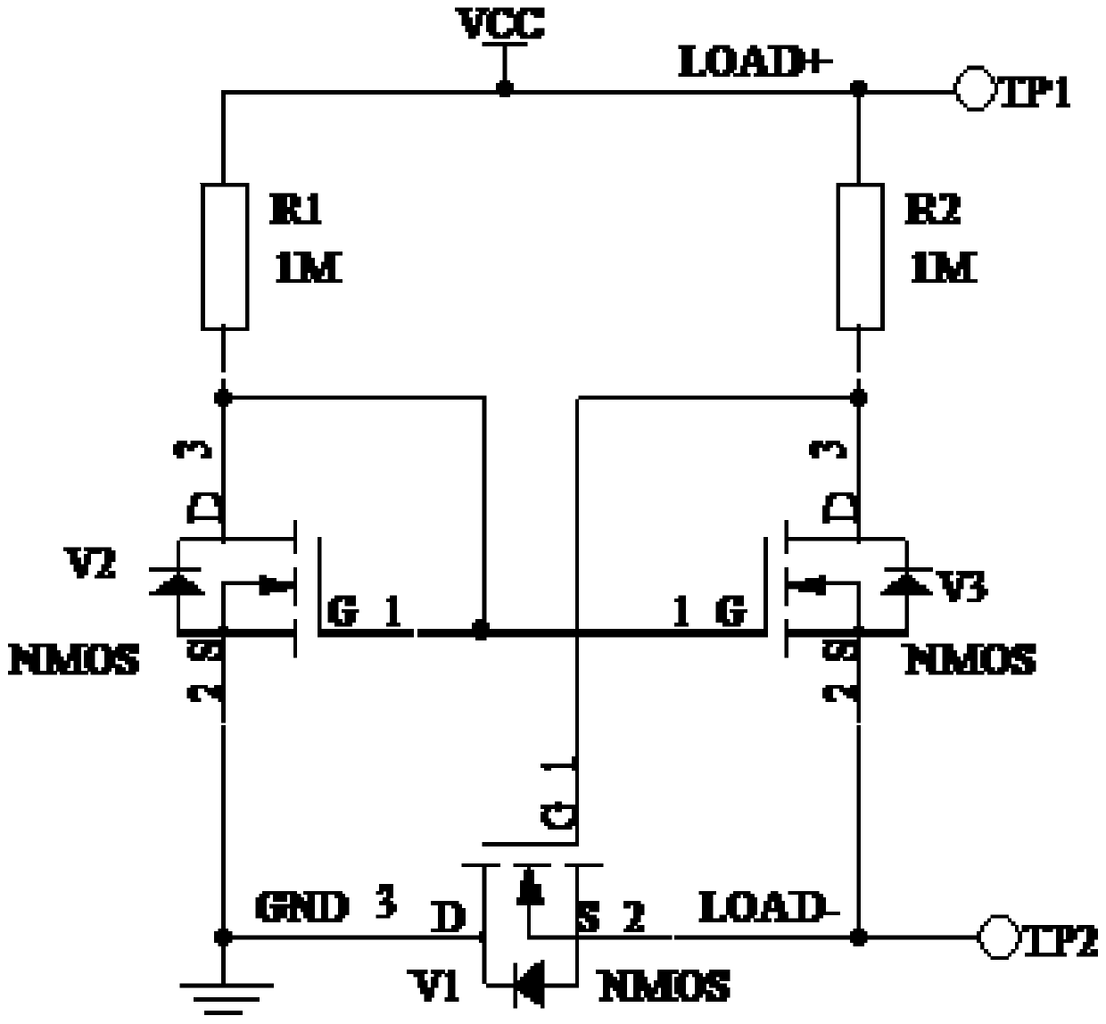
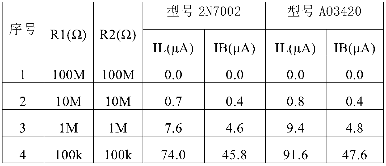
[0028] Such as figure 1As shown, the combinational logic control circuit is composed of two NMOS transistors (V2, V3) of the same type or NMOS pair transistors with the same parameters packaged together, and two serial resistors (R1, R2) to control the NMOS transistors ( V1) conduction and cut-off: when the voltage LOAD- is not less than the voltage GND, the NMOS transistor (V1) is turned on; otherwise, the NMOS transistor (V1) is cut off, preventing the GND current from flowing backward through the NMOS transistor (V1) to LOAD-, protecting LOAD - load circuit. Since the NMOS tube is a voltage device, the current of the NMOS tube is very small when it is turned on and off, and the large resistance resistor connected in series can be ignored. Compa...


PUM


Abstract

The invention discloses an ultralow-loss low-end ideal diode. The ultralow-loss low-end ideal diode comprises a combinational logic control circuit and a first NMOS transistor. The combinational logiccontrol circuit comprises a second NMOS transistor, a third NMOS transistor, a first resistor and a second resistor. The drain electrode of the first NMOS tube is connected with the source electrodeof the second NMOS tube and the negative electrode of the power supply, the source electrode of the first NMOS tube is electrically connected with the source electrode of the third NMOS tube, the gridelectrode of the first NMOS tube is electrically connected with the drain electrode of the third NMOS tube, the grid electrode of the second NMOS tube is connected with the drain electrode of the second NMOS tube and the grid electrode of the third NMOS tube, the drain electrode of the second NMOS tube is connected with the positive electrode of the power supply through the first resistor, the drain electrode of the third NMOS tube is connected with the positive electrode of the power supply through the second resistor, and the load is connected between the positive electrode of the power supply and the source electrode of the first NMOS tube. The anti-backflow circuit has an anti-backflow function, can protect a preceding-stage circuit, and is very low in loss, simple in circuit and highin practicability.

Description

technical field [0001] The invention relates to the technical field of power diodes, in particular to an ultra-low loss low-end ideal diode. Background technique [0002] Due to their unidirectional conduction characteristics, diodes have the function of preventing backflow, and are used more and more. Especially, the power supply connected in series with Schottky diodes has a small voltage drop, and is being welcomed by more and more designers. Since the voltage drop of the Schottky diode is still greater than that of the MOS tube, for some voltage-sensitive circuits, it is more inclined to use a MOS tube with low impedance characteristics to improve the reliability of the product. Now there are many USB power switches (power distribution switches) with built-in functions to prevent backflow, such as the MP62055 chip. Because when an external device is connected to the computer's USB port, the device must not reverse the current flow into the computer's VBus, otherwise it ...

Claims


Application Information

Patent Timeline
Patent Type & Authority Applications(China)
IPC IPC(8): H02M1/088G06F1/26
CPCG06F1/266H02M1/088H02M1/0054Y02B70/10
Inventor 陈石平彭进双
Owner GUANGZHOU AOGE INTELLIGENT TECH CO LTD
Why Eureka
Try Eureka