Through hole filling and plating method applied to optical module high-density interconnection HDI board

A high-density interconnection, optical module technology, applied in the formation of electrical connection of printed components, electrical components, printed circuit manufacturing, etc., can solve problems such as the phenomenon of core wrapping, improve signal transmission stability, prevent core wrapping. Effect

Inactive Publication Date: 2020-05-29
GUANGDONG KINGSHINE ELECTRONICS TECH CO LTD
View PDF7 Cites 6 Cited by
  • Summary
  • Abstract
  • Description
  • Claims
  • Application Information

AI Technical Summary

Problems solved by technology

[0004] In order to solve the above-mentioned technical problem that the core-wrapping phenomenon easily occurs during the filling and plating process of the through-hole of the printed circuit board of the optical module, the present invention provides a method that can increase the copper thickness of the through-hole and prevent the occurrence of the core-wrapping phenomenon for high-density interconnection of optical modules. Through-hole filling and plating method connected to HDI board

Method used


Image

  • Through hole filling and plating method applied to optical module high-density interconnection HDI board

Examples


Embodiment Construction

[0017] The through-hole filling and plating method applied to optical module high-density interconnection HDI boards of the present invention will be further described in detail below in conjunction with specific embodiments and accompanying drawings.

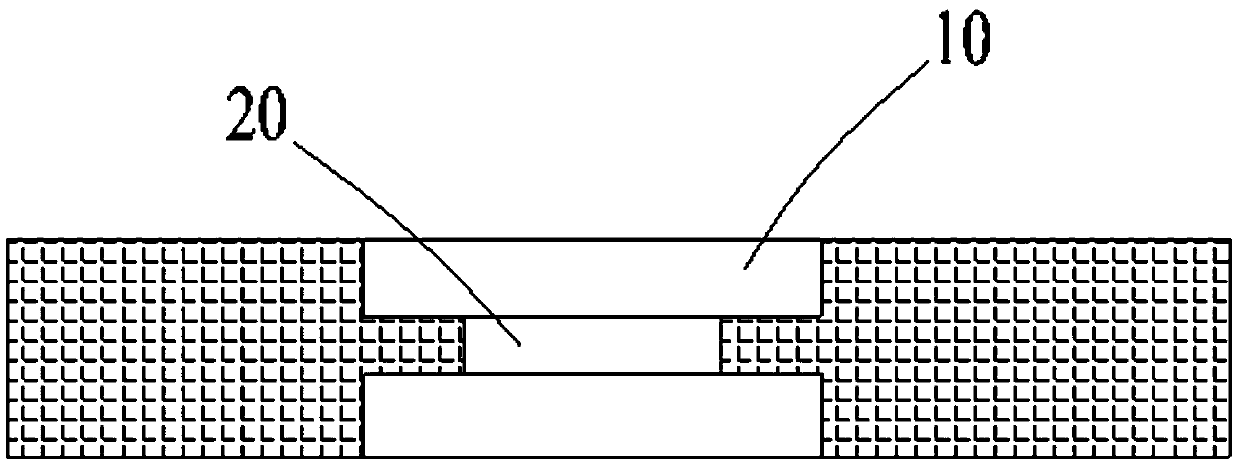
[0018] Please refer to figure 1 As shown, it is a schematic diagram of the structure of the circuit board through hole in the present invention.

[0019] The invention provides a through-hole filling and plating method applied to an optical module high-density interconnection HDI board, which includes the following steps.

[0020] Copper reduction, reduce the surface copper of the circuit board, for example, reduce the surface copper from 1 / 3oz to 6-8μm.

[0021] For front and back drilling, drill holes with the same depth at the same position on the front and back of the circuit board to form the same two blind holes 10, for example, use a 0.2mm drill to turn the hole, and the depth is 0.8mm. Among them, the position of the ...


PUM


Abstract

The invention relates to a through hole filling and plating method applied to an optical module high-density interconnection HDI board. The through hole filling and plating method sequentially comprises the steps of copper reduction, positive and negative drilling, trepanning and drilling, adhesive removal and copper deposition, first exposure and development, through hole electroplating, film stripping, plate grinding, second exposure and development and hole filling and electroplating. According to the through hole filling and plating method applied to the optical module high-density interconnection HDI board, drilling is carried out twice, so that the cross section of a through hole is in the shape of a step which is small at the middle portion and is large at two ends; the step-by-stepfilling and plating of the through hole are achieved through two hole filling steps on the middle portion and the two ends of the through hole; and therefore, the core wrapping phenomenon of the through hole in a filling and plating process is prevented, and the signal transmission stability of the circuit board is effectively improved.

Description

technical field [0001] The invention relates to the technical field of circuit boards, in particular to a through-hole filling and plating method applied to high-density interconnect HDI boards of optical modules. Background technique [0002] The printed circuit board of the optical module generally needs to be powered on for a long time during use, and because the printed circuit board of the optical module is made of high-precision circuits, the through-holes are generally designed with thin copper plating, so that the copper thickness of the entire through-hole is thinner. The overall copper layer has less cross-sectional area. In the case of long-term power on, it is easy to generate a large amount of heat, which will affect the stability of equipment operation. At the same time, the thicker the copper thickness of the through hole, the smaller the impact on the signal transmission between the board layers. [0003] Therefore, in the prior art, the through hole is fill...

Claims


Application Information

Patent Timeline
Patent Type & Authority Applications(China)
IPC IPC(8): H05K3/42
CPCH05K3/42H05K3/423
Inventor 王欣周刚曾祥福
Owner GUANGDONG KINGSHINE ELECTRONICS TECH CO LTD
Why Eureka
Try Eureka