Roll-type GaN-based semiconductor device and preparation method thereof

A semiconductor and device technology, applied in the field of roll-type GaN-based semiconductor devices and their preparation, can solve the problems of increasing process complexity and difficulty in downsizing, and achieve the effect of ensuring heat dissipation performance and simple process

Active Publication Date: 2020-06-02
浙江集迈科微电子有限公司
View PDF4 Cites 0 Cited by
  • Summary
  • Abstract
  • Description
  • Claims
  • Application Information

AI Technical Summary

Problems solved by technology

[0004] In view of the above-mentioned shortcomings of the prior art, the object of the present invention is to provide a roll-type GaN-based semiconductor device and its preparation method, which is used to solve the problem that GaN-based semiconductor devices in the prior art are difficult to meet both the small size of the device and the Without increasing the complexity of the process, it can also ensure the good heat dissipation performance of the device, etc.

Method used


Image

  • Roll-type GaN-based semiconductor device and preparation method thereof
  • Roll-type GaN-based semiconductor device and preparation method thereof
  • Roll-type GaN-based semiconductor device and preparation method thereof

Examples


Embodiment 1

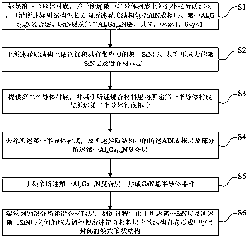
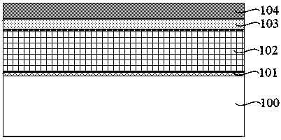
[0043] This embodiment provides a method for preparing a roll-type GaN-based semiconductor device. By forming a SiN layer with tensile stress and a SiN layer with compressive stress, and then cooperate with the process of etching to remove part of the bonding material layer, during the etching process , the two SiN layers with different stresses (tensile stress and compressive stress) are mutually regulated so that the entire semiconductor device is self-rolled into a hollow and closed roll-type tubular structure. This three-dimensional structure meets the small size requirements of the device; at the same time, The GaN-based semiconductor device (rolled tubular structure) formed by self-rolling can be used as a microfluidic channel naturally, without additional post-process for microfluidic channel processing, the process is simple and can ensure the heat dissipation performance of the semiconductor device; moreover, when the semiconductor device is applied Under high temperat...

Embodiment 2

[0071] This embodiment provides a roll-type GaN-based semiconductor device. The semiconductor device can be prepared by the preparation method of the first embodiment above, but is not limited to the preparation method described in the first embodiment, as long as the structure of the semiconductor device can be formed. For the beneficial effects achieved by the semiconductor device, please refer to Embodiment 1, which will not be described in detail below.

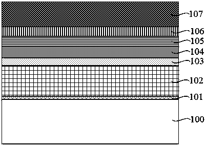
[0072] Such as Figure 8 As shown, the semiconductor device includes:

[0073] a second semiconductor substrate 108;

[0074] a bonding material layer 107 located on the second semiconductor substrate 108;

[0075] A hollow and closed rolled tubular structure 113 is located on the bonding material layer 107. The rolled tubular structure 113 sequentially includes: a second SiN layer 106 with compressive stress, and a first SiN layer with tensile stress. layer 105, the second AlyGa1-yN layer 104, the GaN layer 103 and th...


PUM

PropertyMeasurementUnit
thicknessaaaaaaaaaa
thicknessaaaaaaaaaa
thicknessaaaaaaaaaa

Abstract

The invention provides a roll-type GaN-based semiconductor device and a preparation method thereof. The roll-type GaN-based semiconductor device comprises a second semiconductor substrate, a bonding material layer and a hollow and closed roll-type tubular structure, wherein the hollow and closed roll-type tubular structure comprises two SiN layers with pressure stress and tensile stress, a secondAlyGa<1-y>N layer, a GaN layer and a first AlyGa<1-x>N layer from outside to inside, and x is greater than 0 and less than 1, and y is greater than 0 and less than 1. Two SiN layers with tensile stress and pressure stress are formed, in the sacrificial layer etching process, the SiN layers with different stresses are mutually regulated and controlled to be automatically curled to form the hollow and closed roll-type tubular structure, and the size of the three-dimensional structure is small; meanwhile, the GaN-based semiconductor device formed by self-coiling can be used as a microfluidic channel, the inner surface of the GaN-based semiconductor device is protected by a passivation layer, the process is simple, and the heat dissipation performance of the semiconductor device can be ensured; and a cooling liquid can be introduced into the hollow part of the roll-type tubular structure to dissipate heat of the semiconductor device, so that the heat dissipation performance of the semiconductor device under a high-temperature condition can be ensured.

Description

technical field [0001] The invention belongs to the field of semiconductor device manufacturing, in particular to a roll-type GaN-based semiconductor device and a preparation method thereof. Background technique [0002] As we all know, power electronic systems have always contributed to sustainable development and improved energy conversion rates. As one of the key components of energy conversion in power electronic systems, power semiconductor devices have always been the research focus of many scholars. As a representative of the third-generation semiconductor materials, GaN has a large band gap, high carrier mobility, and high breakdown voltage, and has been identified as a significant candidate for high-voltage, high-power, and high-frequency applications candidate. GaN-based semiconductor devices commonly used in the industry include GaN HEMT devices, GaN FinFETs and nanowire structures. [0003] Existing GaN HEMT devices usually have a planar structure, that is, th...

Claims


Application Information

Patent Timeline
Patent Type & Authority Applications(China)
IPC IPC(8): H01L29/778H01L23/473H01L21/335
CPCH01L23/473H01L29/66462H01L29/778
Inventor 马飞冯光建黄雷
Owner 浙江集迈科微电子有限公司
Why Eureka
Try Eureka