Display panel, display device and manufacturing method of display panel

A technology of display panel and display area, applied in semiconductor/solid-state device manufacturing, semiconductor device, electrical components, etc., can solve the problems of hole halo, EL layer blocking failure, poor packaging effect of display panel, etc., to ensure the effectiveness , The effect of improving the packaging yield

Active Publication Date: 2020-06-05
BOE TECH GRP CO LTD +1
View PDF4 Cites 13 Cited by
  • Summary
  • Abstract
  • Description
  • Claims
  • Application Information

AI Technical Summary

Problems solved by technology

When applying PR glue, the following problems will occur: it is inconvenient to apply PR glue at some positions of the I-shaped spacer column; after the I-shaped spacer column is formed, the PR glue will be applied, and the PR glue will become thinner near the opening, and hole halos will appear. ;When applied to the position of the I-shaped isolation column, air bubbles will be generated at the I-shaped gap, which will cause the PR glue to not cover it
These problems will lead to poor encapsulation of the display panel, failure to block the EL layer, resulting in water and oxygen intrusion, resulting in poor reliability of the display panel

Method used


Image

  • Display panel, display device and manufacturing method of display panel
  • Display panel, display device and manufacturing method of display panel
  • Display panel, display device and manufacturing method of display panel

Examples


Embodiment Construction

[0046] The present invention will be further described in detail below in conjunction with the accompanying drawings and embodiments. It should be understood that the specific embodiments described here are only used to explain related inventions, rather than to limit the invention. It should also be noted that, for ease of description, only parts related to the invention are shown in the drawings.

[0047] It should be noted that, in the case of no conflict, the embodiments of the present invention and the features in the embodiments can be combined with each other. The present invention will be described in detail below with reference to the accompanying drawings and examples.

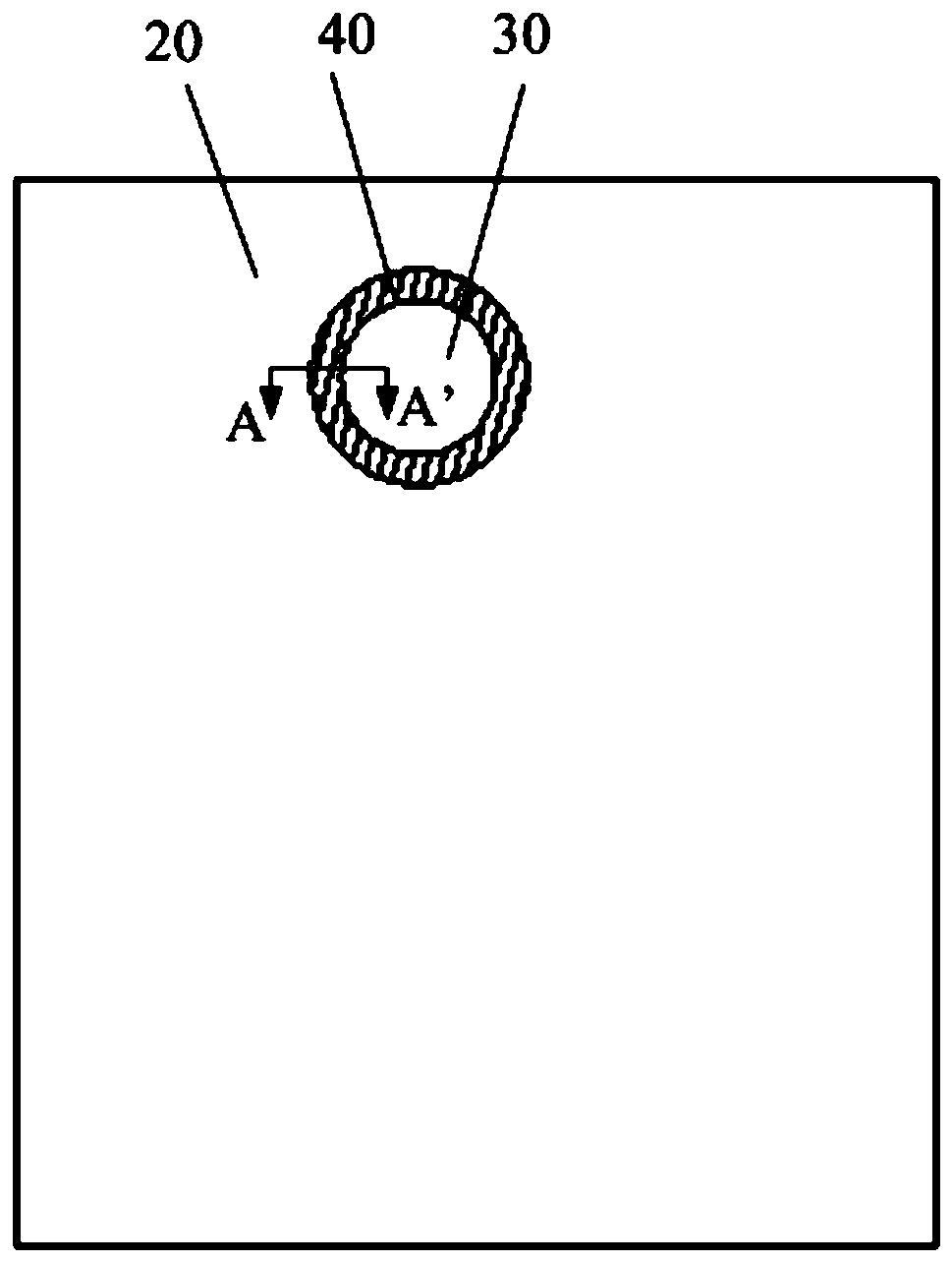
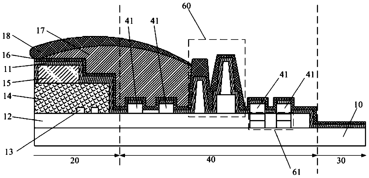
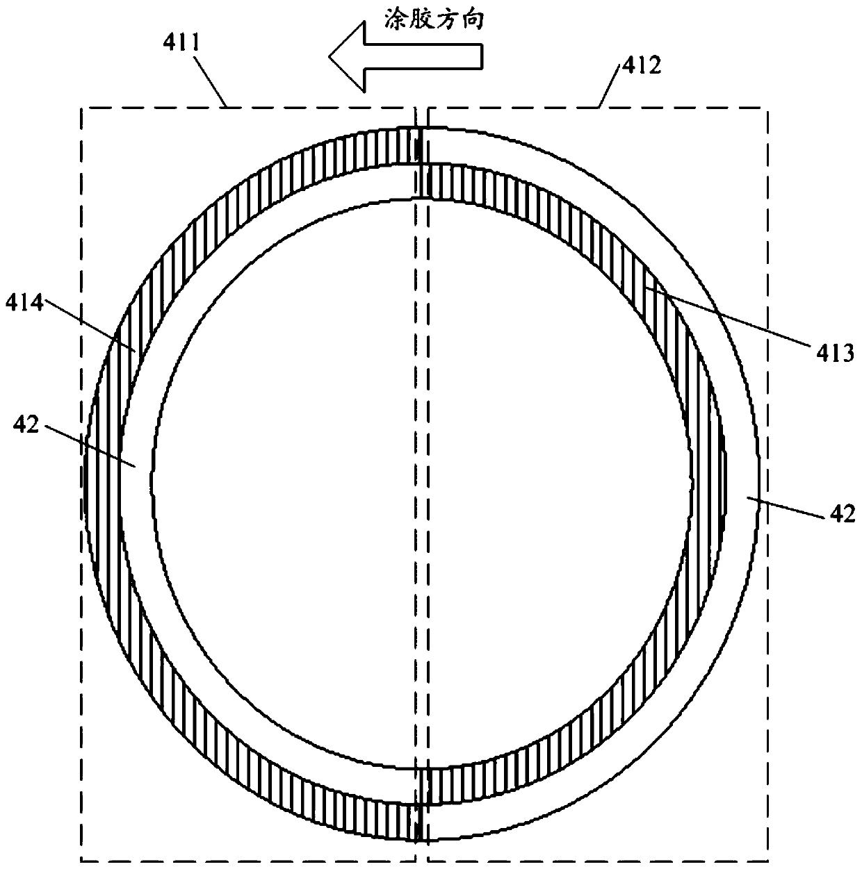
[0048] The full screen refers to a type of display screen with an ultra-high screen-to-body ratio, and an ideal full screen has a screen-to-body ratio of 100%. For example, the front of a mobile phone is all a display interface, but generally limited by the installation needs of basic functional co...


PUM


Abstract

The invention discloses a display panel, a display device and a manufacturing method of the display panel. The display panel comprises a substrate, and the substrate comprises a display area, an opening area and an isolation area located between the display area and the opening area. The isolation area is internally provided with at least one isolation column, each isolation column is arranged around the hole area for a circle, and in the direction parallel to the substrate, each isolation column comprises a first part and a second part which are opposite and connected. The side face, facing the second part, of the first part and the side face, back on to the first part, of the second part are respectively provided with the grooves in a concave manner, and light-emitting layers are arranged in the display area and the isolation area and are disconnected at the grooves. Moreover, the light-emitting layer is of a continuous structure at the side, opposite to the second part, of the firstpart and the side, facing the first part, of the second part. According to the display panel provided by the invention, the packaging yield of the display panel can be effectively improved, and the effectiveness of the isolation column for cutting off a water-oxygen invasion channel is ensured.

Description

technical field [0001] The present invention generally relates to the field of display technology, and in particular to a display panel, a display device and a method for manufacturing the display panel. Background technique [0002] With the development and upgrading of display technology, organic electroluminance display (Organic Electroluminance Display, referred to as: OLED) has gradually become a display device due to its characteristics of self-illumination, high brightness, high contrast, low operating voltage, and flexible display. mainstream products in the field. [0003] At present, OLED display panels are mainly developing in the direction of full screen and narrower borders. For example, most mobile phone manufacturers are pursuing higher screen-to-screen ratios in order to bring users more dazzling visual impact and win market competition. However, for the camera and some sensors, it restricts the development of the screen to a higher screen-to-body ratio. Put...

Claims


Application Information

Patent Timeline
Patent Type & Authority Applications(China)
IPC IPC(8): H01L27/12H01L27/32H01L21/84
CPCH01L27/1218H01L27/1262H10K59/12H10K59/1201
Inventor 周洋刘庭良张鑫和玉鹏郭晓亮刘国栋姜晓峰
Owner BOE TECH GRP CO LTD
Why Eureka
Try Eureka