LED chip

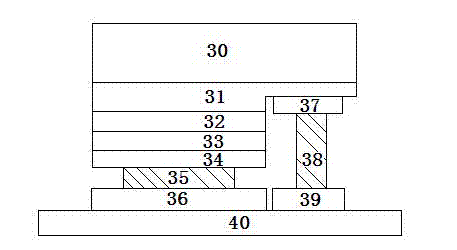
An LED chip, N-type technology, applied in electrical components, circuits, semiconductor devices, etc., can solve the problems of affecting the luminous efficiency of LED chips, the N-level solder layer 38 is too long, affecting the packaging quality rate, etc., to avoid electrode soldering. Or desoldering, increasing the area of ​​the light-emitting area, and improving the effect of the good rate

Active Publication Date: 2013-02-13
启东市天汾电动工具技术创新中心
View PDF3 Cites 8 Cited by
  • Summary
  • Abstract
  • Description
  • Claims
  • Application Information

AI Technical Summary

Problems solved by technology

[0006] 1. The N-type electrode 37 is far away from the P-type electrode 34 in the horizontal direction. The N-type electrode 37 has strict requirements on the position design of the PCB board 27 below it, which affects the packaging quality rate
[0007] 2. The position of the N-type electrode 37 is much higher than that of the P-type electrode 34, resulting in a large gap between it and the PCB board 39 below, and it is easy to make the N-level solder layer 38 too long during soldering, resulting in false soldering or detachment Occurrence of welding
[0008] 3. In order to allow welding of the N-type electrode 37 and the PCB board 39 below it, a large part of the light-emitting area needs to be removed, which affects the luminous efficiency of the LED chip

Method used


Image

  • LED chip
  • LED chip
  • LED chip

Examples


Embodiment Construction

[0078] Combine below Figure 2 to Figure 17 , the present invention is further described:

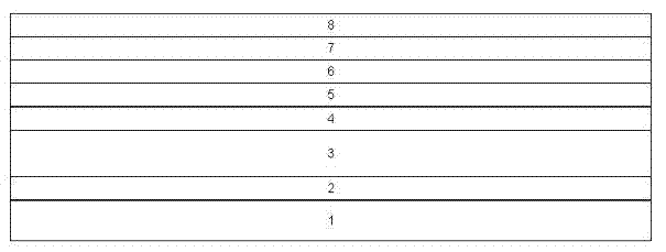
[0079] Such as figure 2 As shown, the substrate 1 is a carrier, generally made of materials such as sapphire, silicon carbide or GaN. Buffer layer 2 is a transitional layer on which high-quality N, P, quantum wells and other materials are grown. LED is composed of pn structure, buffer layer 2, N-type layer 3 layers, N-type confinement layer 4, P-type confinement layer 6 and P-type layer 7 are to form P and N-type materials required for making LED. The light-emitting region layer 5 is the light-emitting region of the LED, and the color of the light is determined by the structure of the active region. P-type ohmic contact layer 8 is the last layer of material growth, and the carrier doping concentration of this layer is relatively high, the purpose is to make smaller ohmic contact resistance. The P-type metal ohmic contact layer is not formed by growth, but by evaporation or sputteri...


PUM


Abstract

The invention relates to an LED chip. The LED chip adopts the structure that an N-type electrode (22) adopts a staircase structure; the lower end of the N-type electrode (22) penetrates an insulating dielectric film (13) to be connected with an N-type layer (3); the middle part of the N-type electrode (22) is attached to the insulating dielectric film (13) at a vertical part; the upper end of the N-type electrode (22) is positioned above the insulating dielectric film (13) at the top, and extends towards the position of a P-type electrode (21); and the upper end of the N-type electrode (22) is connected with a second PCB board (23), and the N-type electrode (22) at the upper end and the P-type electrode (21) are provided with common soldering surfaces of which heights are equal or approximately equal. As the N-type electrode and the P-type electrode of the flip LED chip are provided with the common soldering surfaces of which heights are equal or approximately equal, the yield of packaging in the inverted-chip process of the LED chip is increased, and the phenomenon of inveracious soldering or desoldering of the electrode is avoided.

Description

technical field [0001] The invention relates to an LED chip, in particular to an LED chip with a flip-chip structure. Background technique [0002] The light-emitting surface of the blue, green or violet LED chip made on the sapphire substrate is the growth surface of the epitaxial material, that is, the P-type surface. During the LED packaging process, the sapphire substrate surface is directly fixed on the heat sink. During the working process of the LED, its light-emitting area is the source of heat generation of the device. Since the sapphire substrate itself is an insulator material, and its thermal conductivity is poorer than that of GaN materials, the working current of this formally mounted LED device is limited to ensure the luminous efficiency and working life of the LED. In order to improve the heat dissipation performance of the device, people have designed an LED chip structure, that is, a flip-chip LED chip. [0003] Since the flip chip design was proposed, ...

Claims


Application Information

Patent Timeline
Patent Type & Authority Applications(China)
IPC IPC(8): H01L33/48H01L33/38H01L33/36
Inventor 俞国宏
Owner 启东市天汾电动工具技术创新中心
Why Eureka
Try Eureka