Manufacturing method of LED (light-emitting diode) chip with inverted structure

An LED chip and manufacturing method technology, applied to electrical components, circuits, semiconductor devices, etc., can solve the problems of electrode soldering or de-soldering, low luminous efficiency of chips, etc., so as to increase the packaging yield and avoid electrode soldering or de-soldering. Welding, the effect of reduced area

Inactive Publication Date: 2012-02-15
祝进田
View PDF3 Cites 8 Cited by
  • Summary
  • Abstract
  • Description
  • Claims
  • Application Information

AI Technical Summary

Problems solved by technology

[0005] The present invention designs a manufacturing method of an LED chip with a flip-chip structure, which solves the technical problem that the existing LED chip with a flip-chip structure is prone to defects such as weak soldering or desoldering of electrodes and low luminous efficiency of the chip

Method used


Image

  • Manufacturing method of LED (light-emitting diode) chip with inverted structure
  • Manufacturing method of LED (light-emitting diode) chip with inverted structure
  • Manufacturing method of LED (light-emitting diode) chip with inverted structure

Examples


Embodiment Construction

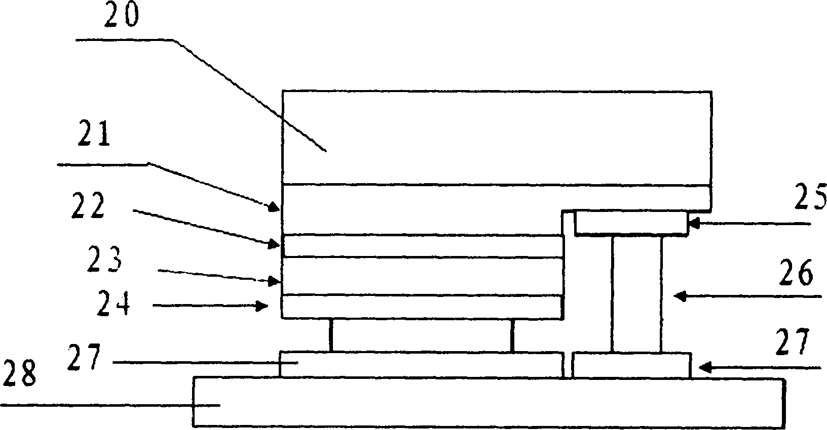
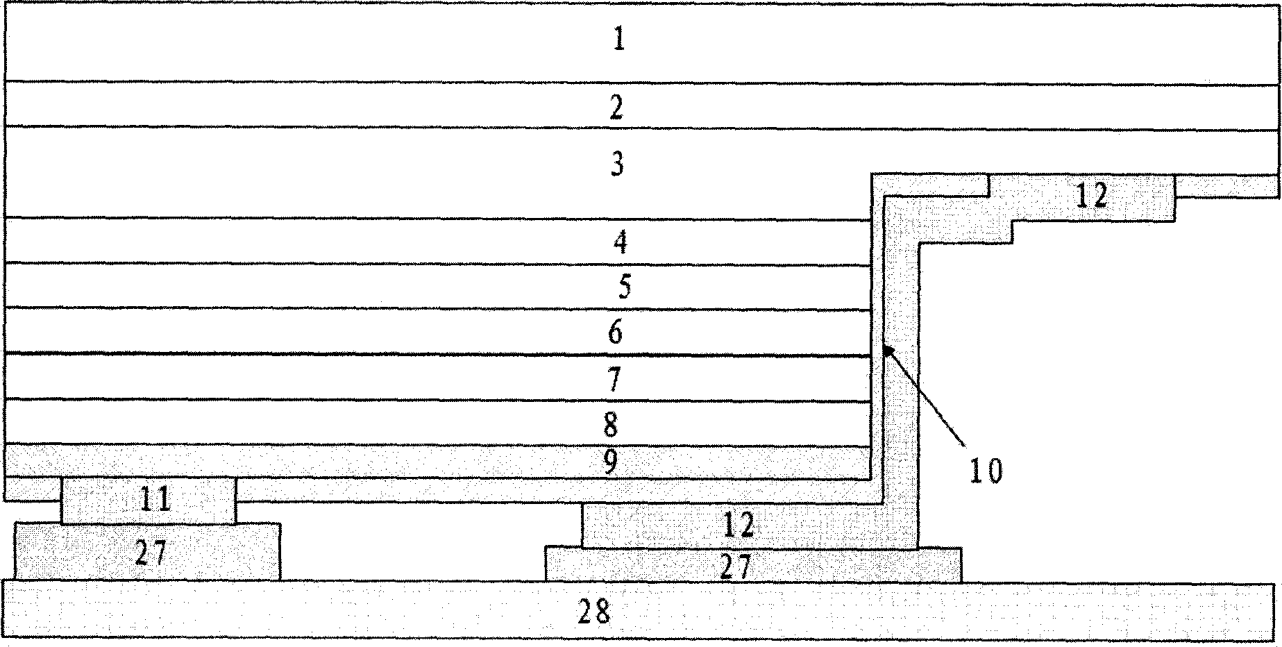
[0019] Combine below figure 2 , To further explain the present invention:

[0020] An LED chip with a flip-chip structure, including an N-type electrode formation area and a P-type electrode formation area. The N-type electrode formation area and the P-type electrode formation area are located on both sides of the LED chip respectively. The N-type electrode formation area is sequentially from top to bottom. Including substrate 1, buffer layer 2, N-type layer 3, N-type confinement layer 4, active area layer 5, P-type confinement layer 6, P-type layer 7, P-type ohmic contact layer 8, light reflection layer 9 And the insulating film 10, one end surface of the N-type electrode 11 passes through the insulating film 10 and is connected to the light reflection layer 9, and the other end surface of the N-type electrode 11 is connected to the heat sink 28 through the PCB board 27; the P-type electrode formation area is from top to The bottom includes the substrate 1, the buffer layer 2,...


PUM


Abstract

The invention relates to a manufacturing method of an LED (light-emitting diode) chip with an inverted structure. The LED chip comprises an N-type electrode formation region and a P-type electrode formation region, wherein the N-type electrode formation region comprises a substrate, a buffer layer, an N-type layer, an N-type respective limiting layer, an active region layer, a P-type respective limiting layer, a P-type layer, a P-type ohmic contact layer, a light reflecting layer and an insulating film; one end face of an N-type electrode passes through the insulating film so as to be connected with the light reflecting layer, and the other end face of the N-type electrode is connected with a heating panel through a PCB (printed circuit board); the P-type electrode formation region comprise a substrate, a buffer layer, an N-type layer and the insulating film, one end of a P-type electrode passes through the insulating film so as to be connected with the N-type layer, and the other end of the P-type electrode is connected with the heating panel by virtue of the PCB; and the two end faces, respectively connected with the PCB, of the N-type electrode and the P-type electrode are positioned at a same horizontal plane. The manufacturing method provided by the invention has the advantages that the N-type electrode and P-type electrode of the LED chip are manufactured in the same surface, the package yield of a chip inversion process is increased, thereby avoiding the occurrence of the electrode rosin joint or sealed-off state.

Description

Technical field [0001] The invention relates to an LED chip structure, in particular to a method for manufacturing an LED chip with a flip-chip structure. Background technique [0002] Generally, the light-emitting surface of the blue, green or violet LED chip fabricated on a sapphire substrate is the growth surface of the epitaxial material, that is, the P-type surface. In the LED packaging process, the sapphire substrate surface is directly fixed on the heat sink. In the working process of the LED, the light-emitting area-the active area is the source of heat generation of the device. Since the sapphire substrate itself is an insulator material, and its thermal conductivity is relatively poor compared to GaN materials, there is a certain limit on the working current of the LED device that is mounted to ensure the luminous efficiency and working life of the LED. In order to improve the heat dissipation performance of the device, a LED chip structure is designed, that is, an LE...

Claims


Application Information

Patent Timeline
Patent Type & Authority Applications(China)
IPC IPC(8): H01L33/00
Inventor 祝进田
Owner 祝进田
Why Eureka
Try Eureka