

Top-emitting light emitting diodes and method of manufacturing thereof
A light-emitting device and interface technology, applied in electrical components, circuits, semiconductor devices, etc., can solve the problems of deterioration of electrical characteristics of light-emitting devices, low luminous efficiency of diodes, lack of highly transparent electrode materials, etc., to improve luminous efficiency and device life, Excellent current-voltage characteristics, the effect of improving ohmic contact characteristics
- Summary
- Abstract
- Description
- Claims
- Application Information
AI Technical Summary
Problems solved by technology
Method used
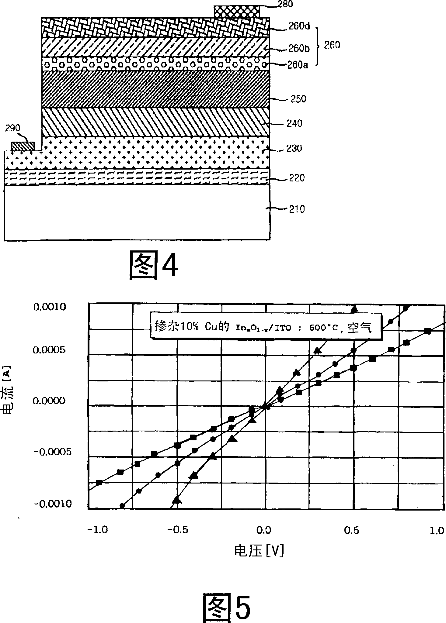
Image

Examples
Embodiment Construction
[0056] Hereinafter, a top emission nitride-based light emitting device according to a preferred embodiment of the present invention will be described in more detail with reference to the accompanying drawings.
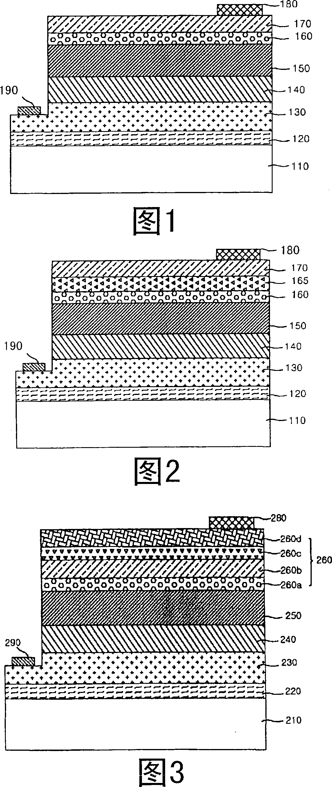
[0057] FIG. 1 shows a cross-sectional view of a top emission nitride-based light emitting device according to a first embodiment of the present invention.
[0058] Referring now to FIG. 1, a top emitting nitride-based light emitting device is formed by a structure comprising a substrate 110, a buffer layer 120, an n-type cladding layer 130, an active layer 140, a p -type cladding layer 150 , interface modification layer 160 and transparent conductive film layer 170 . Reference numerals 180 and 190 denote p-type electrode pads and n-type electrode pads, respectively.
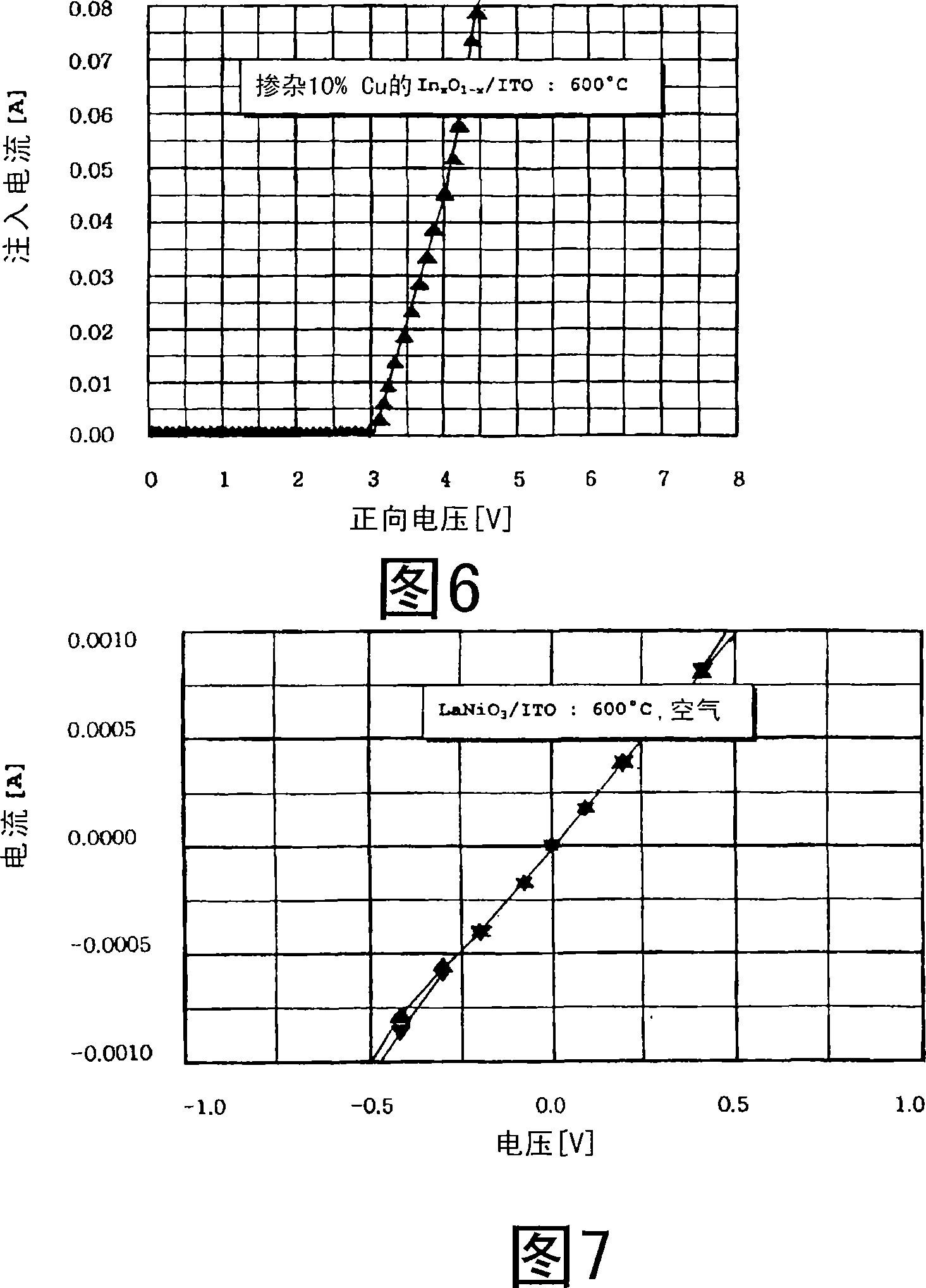
[0059] In addition, the interface modification layer 160 and the transparent conductive film layer 170 stacked on the p-type cladding layer 150 correspond to a multi-ohmic contact layer, that is, a p-typ...
PUM
| Property | Measurement | Unit |
|---|---|---|
| thickness | aaaaa | aaaaa |
| thickness | aaaaa | aaaaa |
| thickness | aaaaa | aaaaa |
Abstract
Description
Claims
Application Information