Cutting device

A cutting device and wafer segmentation technology, which is applied in the manufacture of electrical components, electric solid-state devices, semiconductor/solid-state devices, etc., can solve the problems of high equipment cost, and achieve the effect of reducing equipment cost and realizing space saving.

Pending Publication Date: 2020-06-09
DISCO CORP
View PDF1 Cites 2 Cited by
  • Summary
  • Abstract
  • Description
  • Claims
  • Application Information

AI Technical Summary

Problems solved by technology

[0006] In the past, it was necessary to have a dicing device for dividing a wafer into individual device chips and an ultraviolet irradiation device for irradiating ultraviolet rays to an adhesive tape, and there were problems in that installation space for each device was required and equipment costs became expensive.

Method used


Image

  • Cutting device
  • Cutting device
  • Cutting device

Examples


Embodiment Construction

[0023] Hereinafter, a cutting device according to an embodiment of the present invention will be described in detail with reference to the drawings.

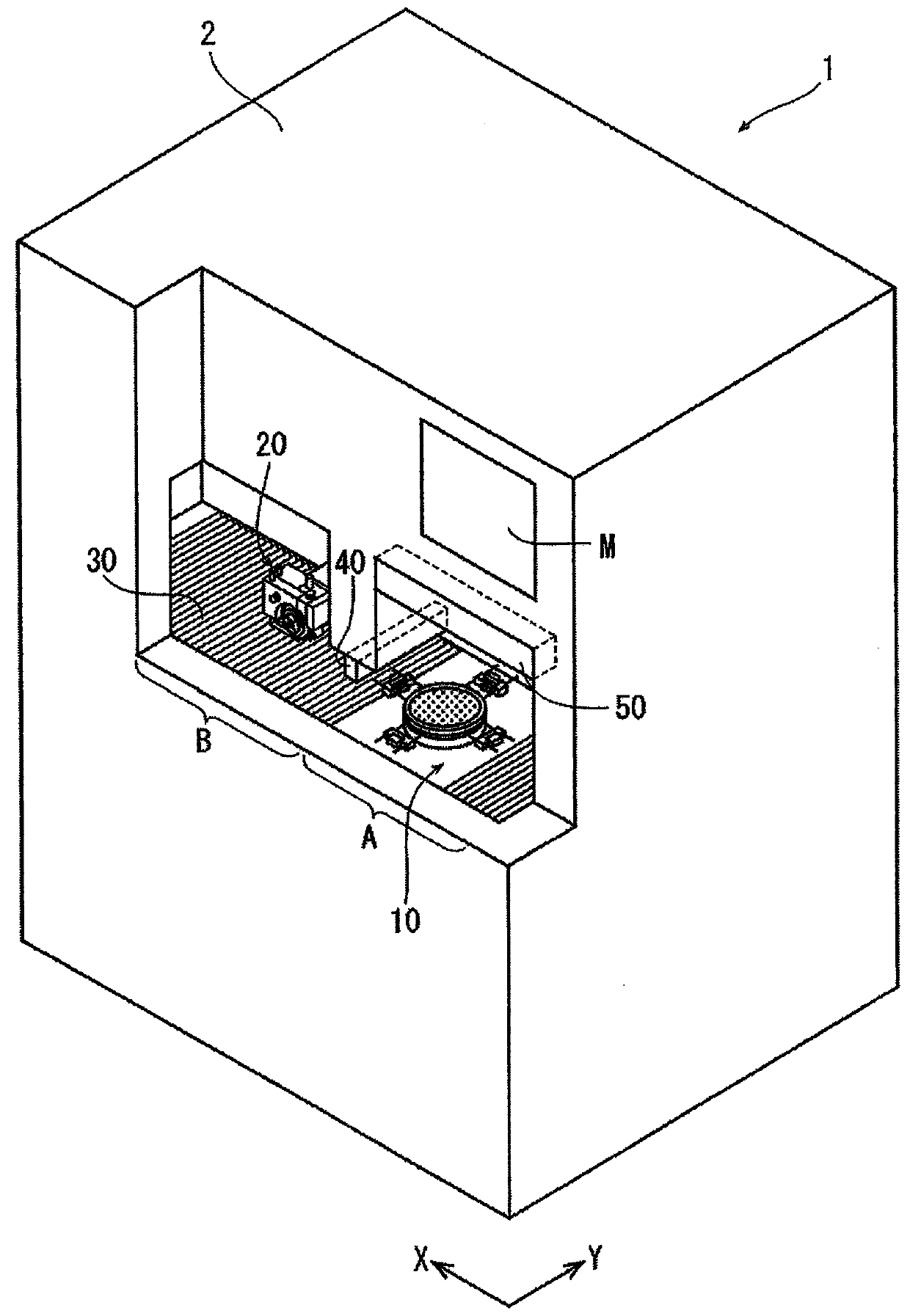
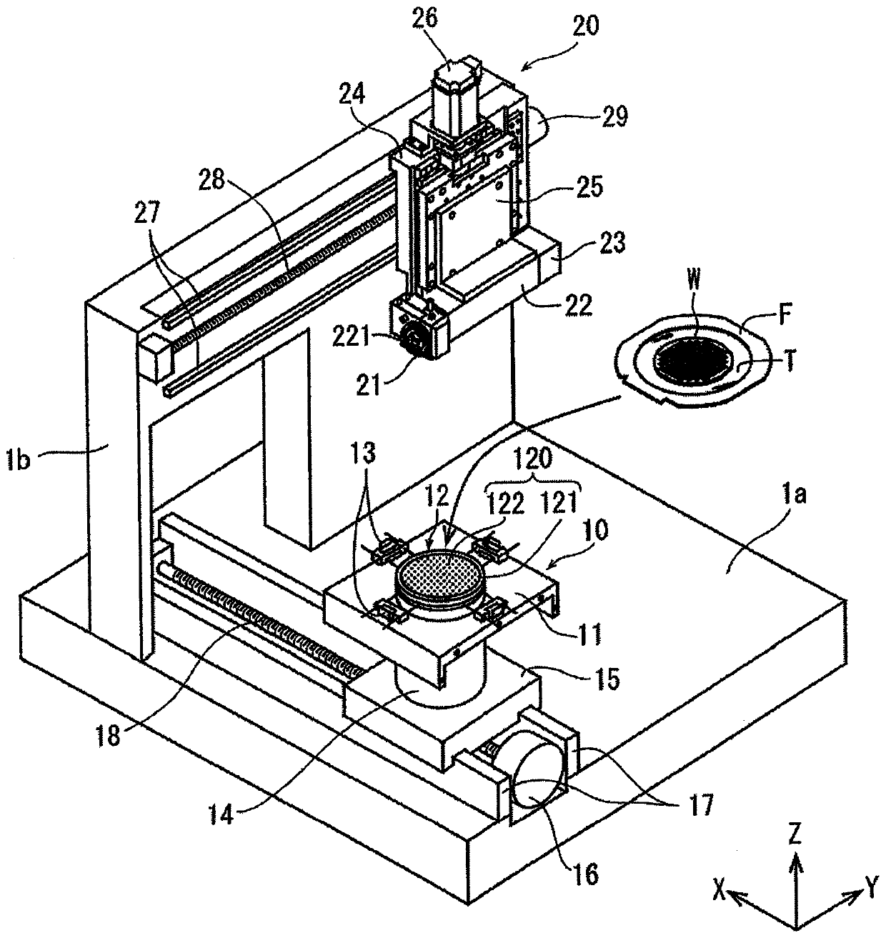
[0024] exist figure 1 shows an overall perspective view of the cutting device 1 of this embodiment, and figure 2 shown in figure 1 A perspective view of the main parts of the cutting device 1 is shown.

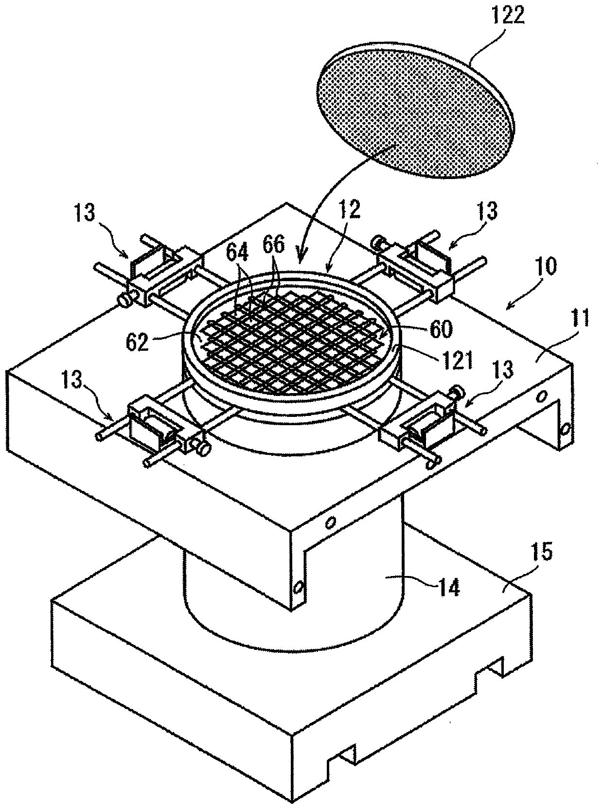
[0025] The cutting device 1 has the ability to place and hold the workpiece ( figure 2 The chuck table 10 of the wafer W) shown also has a cutting unit 20 for dividing the wafer W supported by the ring frame F via the respective adhesive tapes T into individual device chips.

[0026] Such as figure 1 As shown, the chuck table 10 can advance and retreat in the X-axis direction shown by the arrow X to be positioned in the loading and unloading area A and the processing area B. In the loading and unloading area A, a wafer W or wafer W is placed and held on the chuck table 10. The chipped wafer W is taken out from the chuck t...


PUM


Abstract

Provided is a cutting device capable of saving space and suppressing equipment costs when processing requiring a cutting device and an ultraviolet irradiation device is performed. The cutting device divides a wafer supported on an annular frame through an adhesive tape into individual device chips. The cutting device includes: a chuck table including a wafer support table that supports the wafer and a frame support portion (13) that is disposed on an outer periphery of the wafer support table and supports the annular frame; and a cutting unit that performs cutting processing on the wafer supported by the wafer supporting table. The wafer support table includes an ultraviolet irradiation unit that irradiates ultraviolet light to reduce an adhesive force of the adhesive tape in a region corresponding to the wafer.

Description

technical field [0001] The present invention relates to a dicing device for dividing a wafer supported by an annular frame via an adhesive tape into individual device chips. Background technique [0002] The wafer divided by a plurality of intersecting dividing lines and formed with multiple devices such as ICs and LSIs on the front surface is divided into individual device chips by a dicing device, and the divided device chips are used in electronic equipment such as mobile phones and personal computers ( For example, refer to Patent Document 1). [0003] In addition, before the wafer is divided into individual device chips, the wafer is positioned at the opening of the annular frame having the opening for housing the wafer, and the adhesive tape is attached together with the annular frame to form an integral body. [0004] In addition, after the wafer is diced to be divided into individual device chips, the area of ​​the adhesive tape corresponding to the wafer is irradia...

Claims


Application Information

Patent Timeline
Patent Type & Authority Applications(China)
IPC IPC(8): H01L21/304H01L21/683H01L21/687H01L21/78
CPCH01L21/78H01L21/304H01L21/6836H01L21/68785H01L2221/68327H01L2221/68386
Inventor 姚龙才马路良吾
Owner DISCO CORP
Why Eureka
Try Eureka