Upgrading method of fpga based on pcie interface
A technology for upgrading commands and connection status, applied in the field of communication, which can solve problems such as business impact, and the host is prone to downtime or restart.
- Summary
- Abstract
- Description
- Claims
- Application Information
AI Technical Summary
Problems solved by technology
Method used
Image


Examples
Embodiment 1
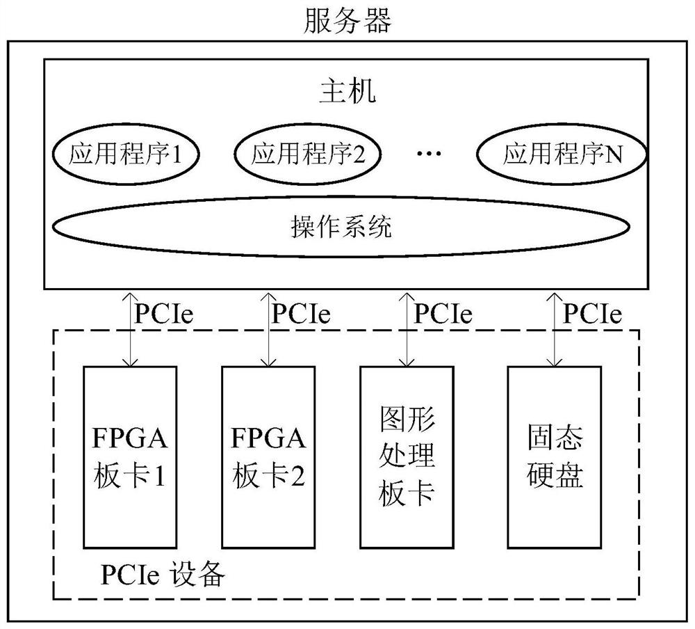
[0058] This embodiment introduces an FPGA upgrade method based on an application scenario where an FPGA board is connected to a host through a PCIe slot. see Figure 5 , which is a structural block diagram of the application scenario of this embodiment, based on Figure 5 , the execution process of the host side and the FPGA board side will be introduced in detail below.
[0059] see Figure 6 , is a flow chart of the host side, and each method step in the process can be specifically executed by a processor (such as a CPU) in the host by reading instructions in the memory in a software manner, and the software can be a production FPGA board Provided by the manufacturer, it is used to provide an upgrade program for upgrading the FPGA board. The upgrade program can be a third-party application program (that is, an application program that is not included with the operating system, but is installed after the operating system is installed) , of course, may also be a program tha...
Embodiment 2
[0120] Based on the above embodiments, this embodiment discloses another FPGA upgrade method, see Figure 9 , which is a hardware architecture diagram based on this embodiment. The difference between this embodiment and the first embodiment is that the FPGA and the host may not judge the state of each other by detecting the change of the PCIe link state, but interact through reserved physical pins. Among them, there may be two reserved pins, one of which is used for communication from the host to the FPGA; the other is used for communication from the FPGA to the host. The reserved pin can also be a pin capable of two-way communication. The pin can be used by time-division multiplexing, that is, it is used for communication from the host to the FPGA at a certain time, and used for communication at another time. Communication from the FPGA to the host. The following process is described based on the situation of two pins.
[0121] Some steps in this embodiment are similar to ...
Embodiment 3
[0147] Based on the second embodiment, this embodiment provides another FPGA upgrade method. In this embodiment, S102 in the second embodiment may be executed first, then S104 is executed, and then S103 is executed. Correspondingly, in this case, the FPGA does not need to wait for a preset time, but can directly start the upgrade.
[0148] The specific implementation methods of the host computer and the FPGA are introduced respectively below.
[0149] see Figure 12 , is a flow chart of processing on the host side, and each step is executed by the host, including:
[0150] S121. Load new configuration data into the FPGA configuration memory.
[0151]S122. Suspend one or more application programs that use the PCIe link to access the FPGA, and save the scene.
[0152] S123. Uninstall the PCIe driver corresponding to the FPGA.
[0153] S124. Send an upgrade instruction to the FPGA.
[0154] At this time, because the PCIe driver is uninstalled, the upgrade command cannot be s...
PUM
 Abstract
Description
Claims
Application Information