Fan-out type wafer level packaging structure and manufacturing method thereof

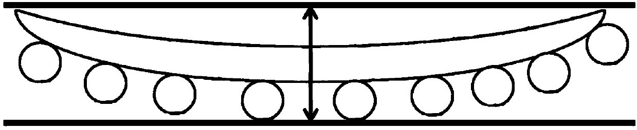
A technology of wafer-level packaging and manufacturing methods, which is applied in semiconductor/solid-state device manufacturing, semiconductor/solid-state device components, semiconductor devices, etc., can solve the problem that the structure is easy to warp and increase the difficulty of the ball pin process of the redistribution layer , large differences in thermal expansion coefficients, etc., to reduce the difficulty of the process, reduce the size of the package structure, and reduce the warpage.

Pending Publication Date: 2020-06-12
CHANGXIN MEMORY TECH INC
View PDF0 Cites 0 Cited by
  • Summary
  • Abstract
  • Description
  • Claims
  • Application Information

AI Technical Summary

Problems solved by technology

Due to the large difference in thermal expansion coefficient between the plastic sealing layer and the die, the overall structure is prone to warping after the plastic sealing layer is formed, which increases the difficulty of forming the redistribution layer and the ball pin process

Method used


Image

  • Fan-out type wafer level packaging structure and manufacturing method thereof
  • Fan-out type wafer level packaging structure and manufacturing method thereof
  • Fan-out type wafer level packaging structure and manufacturing method thereof

Examples


Embodiment Construction

[0023] The following is a specific example to illustrate the implementation of the "manufacturing method of fan-out wafer level packaging structure" and "fan-out wafer level packaging structure" disclosed in the present invention. Those skilled in the art can learn from this specification The disclosed content understands the advantages and effects of the present invention. The present invention can be implemented or applied through other different specific embodiments, and various modifications and changes can be made to the details in this specification based on different viewpoints and applications without departing from the concept of the present invention. The following embodiments will further describe the relevant technical content of the present invention in detail, but the disclosed content is not intended to limit the protection scope of the present invention.

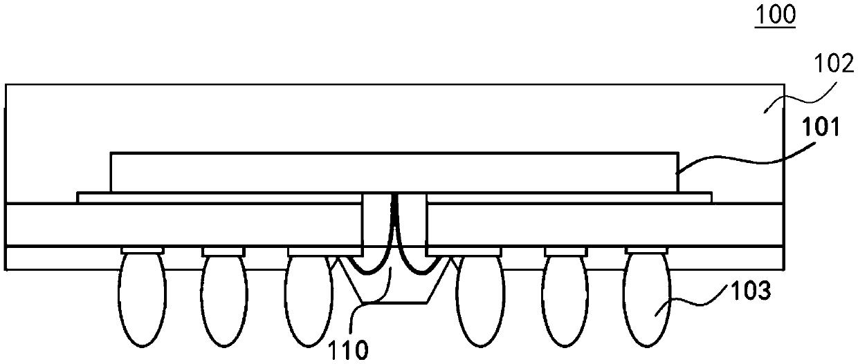
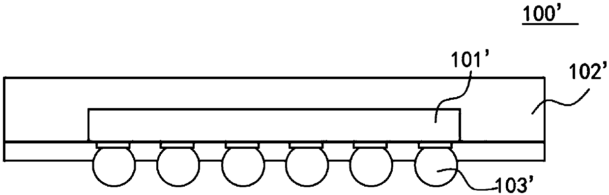
[0024] The invention provides a method for manufacturing a fan-out wafer level packaging structure. see ...


PUM

PropertyMeasurementUnit
thicknessaaaaaaaaaa
thicknessaaaaaaaaaa
thicknessaaaaaaaaaa

Abstract

The invention provides a fan-out type wafer level packaging structure and a manufacturing method thereof, and the method comprises the steps: providing a support wafer layer, and forming an adhesive layer on the support wafer layer; bonding a plurality of bare chipsto the surface of the adhesive layer, the bare chipshaving pins facing the adhesive layer surface; forming a pre-cured layer on the adhesive layer and sides, far away from the support wafer layer, of the bare chips, wherein the pre-cured layer covers the bare chips; forming a curing layer on one side, far away from the support waferlayer, of the pre-curedlayer; removing the support wafer layer and the adhesive layer to expose pins of the bare chips; forming a rewiring layer on the surfaces of one sides of the exposed pins of the bare chips, and forming spherical pins on the rewiring layer; polishing the cured layer to a predetermined thickness; cutting to form a fan-out type wafer level packaging structure; wherein the curedlayer and the pre-curedlayer have different thermal expansion coefficients, and the curedlayer and the bare chips have the same thermal expansion coefficient. The packaging structure produced by themethod reduces warping of the wafer in a fan-out wafer level packaging process.

Description

technical field [0001] The invention relates to the field of semiconductor chip packaging, in particular to a fan-out wafer-level packaging structure and a manufacturing method thereof. Background technique [0002] In the development process of the dynamic random access memory (DRAM, Dynamic Random Access Memory) manufacturing process, in the related art, the DRAM packaging structure 100 (such as Figure 1A shown) for packaging, including a die 101 , a plastic encapsulation layer 102 and pins 103 . For the opening 110 , the design of the position of the pad on the die 101 has strict requirements, and needs to match the manufacturing capability of the substrate factory. In addition, the WBGA DRAM packaging structure needs to transmit signals through the substrate, and there are strict requirements on the thickness of the DRAM packaging structure and the metal wiring lines in the substrate. [0003] The fan-out wafer-level packaging structure in the related art (such as Fi...

Claims


Application Information

Patent Timeline
Patent Type & Authority Applications(China)
IPC IPC(8): H01L21/60H01L21/56H01L23/488H01L23/482H01L23/29H01L23/31H01L25/065
CPCH01L24/02H01L24/17H01L25/0655H01L23/3107H01L23/293H01L21/56H01L24/03H01L24/80H01L2224/02331H01L2224/02379H01L2224/03H01L2224/0231H01L2224/17107H01L2224/80862H01L2224/97H01L2224/18H01L2224/12105H01L2924/3511
Inventor 范增焰吕开敏全昌镐
Owner CHANGXIN MEMORY TECH INC
Why Eureka
Try Eureka