OLED screen punching method

A screen and hole area technology, applied in the field of OLED screen punching, can solve the problems of component failure, difficult fine patterning, large investment, etc., and achieve the effect of low cost and simple operation

Active Publication Date: 2020-06-16
BOE TECH GRP CO LTD +1
View PDF6 Cites 13 Cited by
  • Summary
  • Abstract
  • Description
  • Claims
  • Application Information

AI Technical Summary

Problems solved by technology

[0003] The mainstream solution for the under-display camera is to dig holes in the display functional area to place the camera. However, when the functional area is provided with holes, it is difficult to pattern finely because the organic light-emitting layer and other layers are tiled on the entire surface. These layers will become the introduction path of oxygen or moisture or the propagation path of fine cracks, resulting in component failure, so a solution is required
A common solution is laser ablation, but this solution requires sophisticated laser system equipment and requires a large investment

Method used


Image

  • OLED screen punching method
  • OLED screen punching method
  • OLED screen punching method

Examples


Embodiment Construction

[0020] The application will be further described in detail below in conjunction with the accompanying drawings and embodiments. It should be understood that the specific embodiments described here are only used to explain related inventions, rather than to limit the invention. It should also be noted that, for ease of description, only parts related to the invention are shown in the drawings.

[0021] It should be noted that, in the case of no conflict, the embodiments in the present application and the features in the embodiments can be combined with each other. The present application will be described in detail below with reference to the accompanying drawings and embodiments.

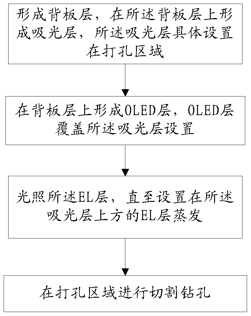
[0022] Please refer to figure 1 , the present embodiment provides a method for punching holes in an OLED screen, comprising the steps of:

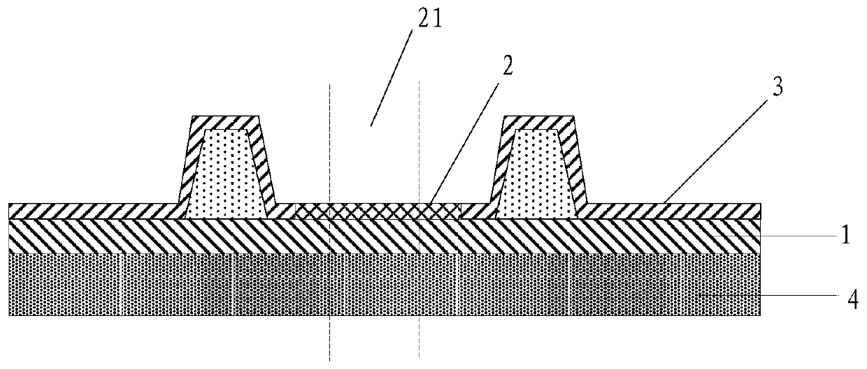
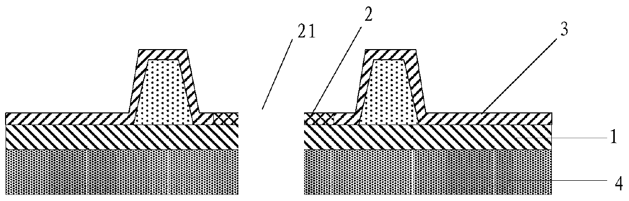
[0023] Forming a backplane layer 1, forming a light-absorbing layer 2 on the backplane layer 1, and the light-absorbing layer 2 is specifically arranged in t...


PUM


Abstract

The invention discloses an OLED screen punching method, which comprises the steps of forming a backboard layer, and forming a light absorption layer on the backboard layer, wherein the light absorption layer is specifically arranged in a punching area; forming an OLED layer on the backboard layer, wherein the OLED layer covers the light absorption layer; illuminating the OLED layer until the OLEDlayer arranged above the light absorption layer is evaporated; and conducting cutting and drilling in the punching area. According to the technical scheme provided by the embodiment of the invention,the light absorption layer is arranged at the punching position, the OLED layer material in the screen punching area is removed through illumination, the periphery of the punching area is covered by the light absorption layer, so that the water and oxygen permeation path of the punching area is blocked through the light absorption layer, oxygen or moisture cannot enter or spread through the OLED layer, the condition of component failure does not occur, and the punching scheme is simple to operate and relatively low in cost.

Description

technical field [0001] The invention generally relates to the field of display, and in particular to a method for punching holes in an OLED screen. Background technique [0002] In the past two years, the development of full-screen screens has been booming, and the pursuit of higher and higher screen-to-body ratios requires solving the problem of setting up the front camera. This design is Sharp's beauty point. Nowadays, the emergence of under-screen fingerprint technology and earpiece hidden design has made the full-screen technology more mature, and the water drop screen has emerged as the times require, so hiding the camera has become the last problem. [0003] The mainstream solution for the under-display camera is to dig holes in the display function area to place the camera. However, when openings are set in the function area, it is difficult to pattern finely because the organic light-emitting layer and other layers are tiled on the entire surface. These layers will...

Claims


Application Information

Patent Timeline
Patent Type & Authority Applications(China)
IPC IPC(8): H01L51/56H01L51/52H01L27/32
CPCH10K59/65H10K59/10H10K50/844H10K71/00Y02E10/549
Inventor 张振华王本莲唐国强孙阔
Owner BOE TECH GRP CO LTD
Why Eureka
Try Eureka