
Bulk acoustic wave filter element and forming method thereof, multiplexer and communication equipment
A bulk acoustic wave filter and filter technology, which is applied in the field of filters, can solve problems such as occupation and the space occupied by the bulk acoustic wave filter is difficult to reduce, and achieve the effects of reducing the plane area, reducing the volume, and improving the roll-off performance
- Summary
- Abstract
- Description
- Claims
- Application Information
AI Technical Summary
Problems solved by technology
Method used
Image

Examples
Embodiment Construction
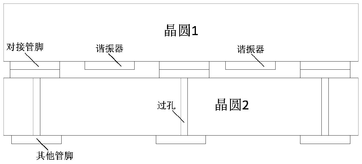
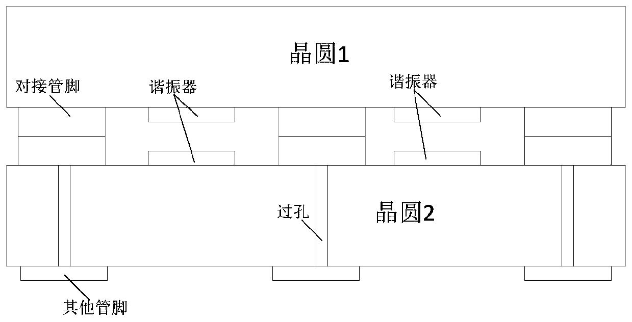
[0055] figure 2 is a cross-sectional view of a bulk acoustic wave filter element provided by an embodiment of the present invention, figure 2In the above, the resonator resonator is manufactured on both the upper wafer (wafer 1) and the lower wafer (wafer 2), and the wafer 1 and wafer 2 are bonded through the butt pin PAD to form a filter. The resonators on wafer 1 and the resonators on wafer 2 need to meet certain spacing requirements to adjust the capacitance between the resonators, so as to realize the adjustment of the equivalent kt of the resonators, and then ensure certain performance requirements. Specifically, the spacing D needs to satisfy 0<D≤50um (micrometer), and more specifically, D needs to satisfy 1um≤D≤10um.
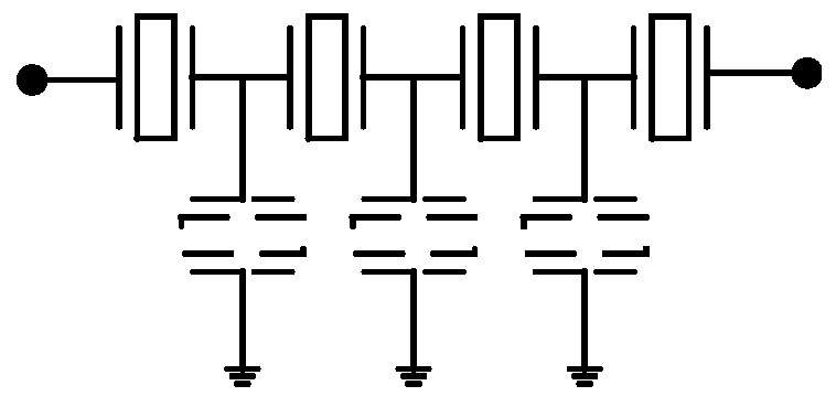
[0056] image 3 is an arrangement mode of a resonator according to an embodiment of the present invention, image 3 In the figure, the solid line is a series resonator, which can be set on wafer 1 or wafer 2. On the contrary, the parallel resonator i...
PUM
 Abstract
Description
Claims
Application Information