Chuck plate, chuck structure having chuck plate, and bonding device having chuck structure

A chuck structure and chuck plate technology, which is applied in the manufacture of electrical components, circuits, semiconductors/solid-state devices, etc., can solve problems such as low vacuum adsorption force, wafers cannot be completely attached to chuck structures, etc., and reduce welding defects rate effect

Pending Publication Date: 2020-06-26
MICOCERAMICS LTD
View PDF7 Cites 1 Cited by
  • Summary
  • Abstract
  • Description
  • Claims
  • Application Information

AI Technical Summary

Problems solved by technology

Therefore, the vacuum adsorption force at the edge of the chuck structure is relatively low, and the wafer cannot be completely attached to the chuck structure.

Method used


Image

  • Chuck plate, chuck structure having chuck plate, and bonding device having chuck structure
  • Chuck plate, chuck structure having chuck plate, and bonding device having chuck structure
  • Chuck plate, chuck structure having chuck plate, and bonding device having chuck structure

Examples


Embodiment Construction

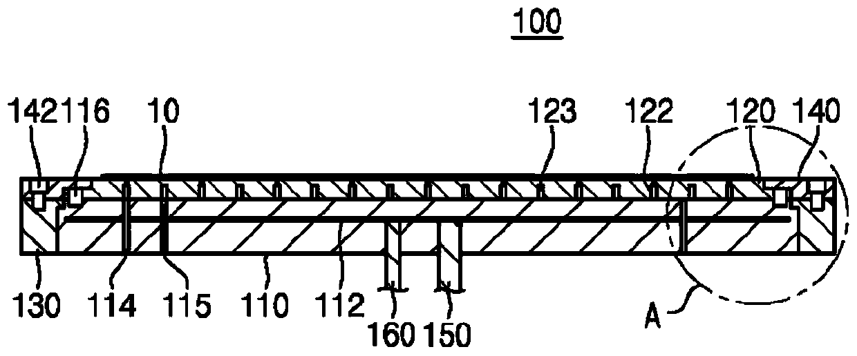
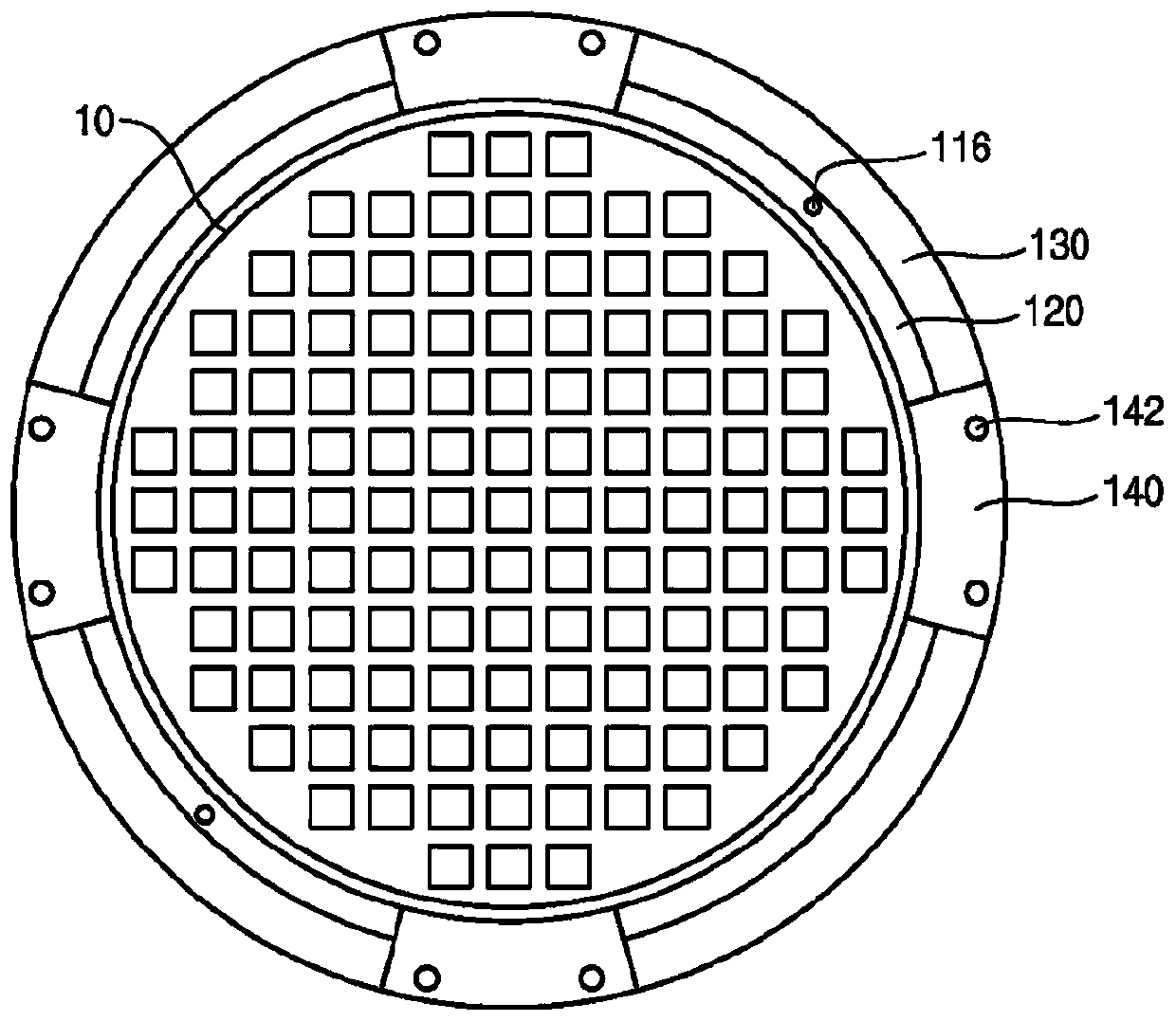
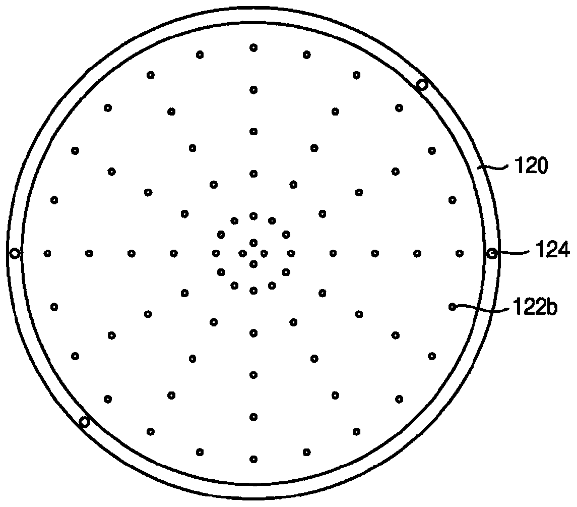
[0047] The chuck plate, the chuck structure with the chuck plate and the welding device with the chuck structure according to the embodiments of the present invention will be described in detail below with reference to the accompanying drawings. The present invention can be modified variously and can have various forms, and specific embodiments are shown by way of example in the drawings and described in detail in the text. However, this is not intended to limit the present invention to a specific disclosed form, and it should be understood that all changes, equivalents, and substitutions included within the idea and technical scope of the present invention are included. In describing each figure, similar reference numerals are used for similar constituent elements. In the drawings, in order to contribute to the clarity of the present invention, the size of the structural objects is shown enlarged than the actual size.

[0048] Terms such as first and second may be used to de...


PUM

PropertyMeasurementUnit
Thermal conductivityaaaaaaaaaa

Abstract

A chuck plate of a chuck structure is placed on a heating plate, supports a wafer on the upper surface thereof, transfers, to the wafer, heat generated by the heating plate such that the wafer is heated, and can have: vacuum holes penetrating the top and the bottom thereof in order to adsorb the wafer by vacuum force; and a vacuum groove, which is provided on the lower surface thereof such that the chuck plate is vacuum-adsorbed to the heating plate, and forms a space by being limited by the upper surface of the heating plate.

Description

technical field [0001] The present invention relates to a chuck plate, a chuck structure with the chuck plate, and a welding device with the chuck structure. More specifically, it relates to a chuck plate for fixing a wafer, with the chuck A plate chuck structure and a welding device having the chuck structure. Background technique [0002] Recently, in order to meet the demand for miniaturization of electronic components such as semiconductor packages, a technology of stacking a plurality of electronic components to form a stacked die package has been developed. [0003] The stacked die package can achieve high integration as a semiconductor package in which dies are stacked on a package substrate. The stacked die package is manufactured at a chip level or a wafer level. [0004] In order to fabricate a stacked die package at said die level or wafer level, perform the operations required to apply heat and pressure and solder die to die or die to die or die to die, the ope...

Claims


Application Information

Patent Timeline
IPC IPC(8): H01L21/683H01L21/67H01L21/687
CPCH01L21/67H01L21/683H01L21/687H01L21/6838H01L21/67103H01L21/68721H01L21/6835
Inventor 南成龙郑仁荣
Owner MICOCERAMICS LTD
Why Eureka
Try Eureka