Semiconductor detection device

A detection device and semiconductor technology, which is applied in sorting and other directions, can solve the problems of unclassified detection results and low automation of semiconductor detection, and achieve the effect of facilitating later operations

Inactive Publication Date: 2020-06-30
苏州埃尔森自动化设备有限公司
View PDF12 Cites 4 Cited by
  • Summary
  • Abstract
  • Description
  • Claims
  • Application Information

AI Technical Summary

Problems solved by technology

[0005] In view of the above-mentioned shortcomings of the prior art, the object of the present invention is to provide a semiconductor inspection device, which is used to solve the problems in the prior art that the automation of semiconductor inspection is low and the inspection results cannot be classified.

Method used


Image

  • Semiconductor detection device
  • Semiconductor detection device
  • Semiconductor detection device

Examples


Embodiment Construction

[0032] The implementation of the present invention will be illustrated by specific specific examples below, and those skilled in the art can easily understand other advantages and effects of the present invention from the contents disclosed in this specification.

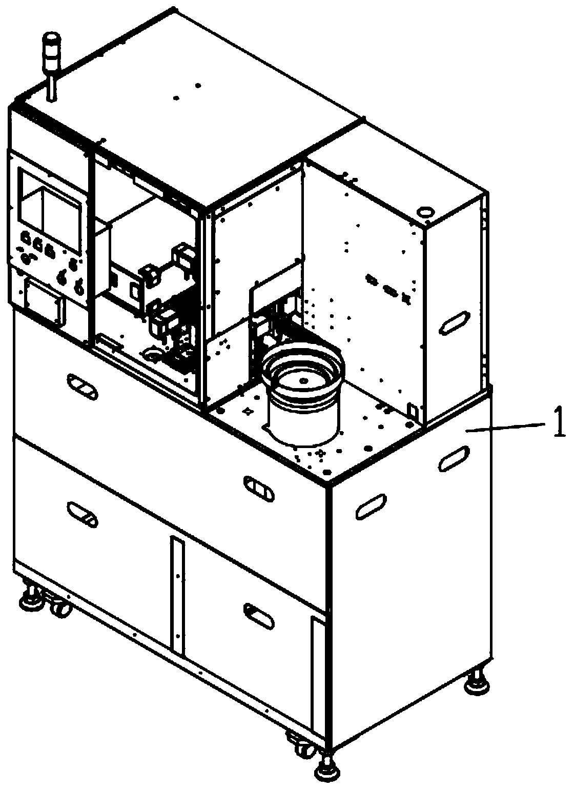
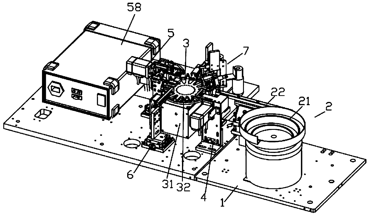
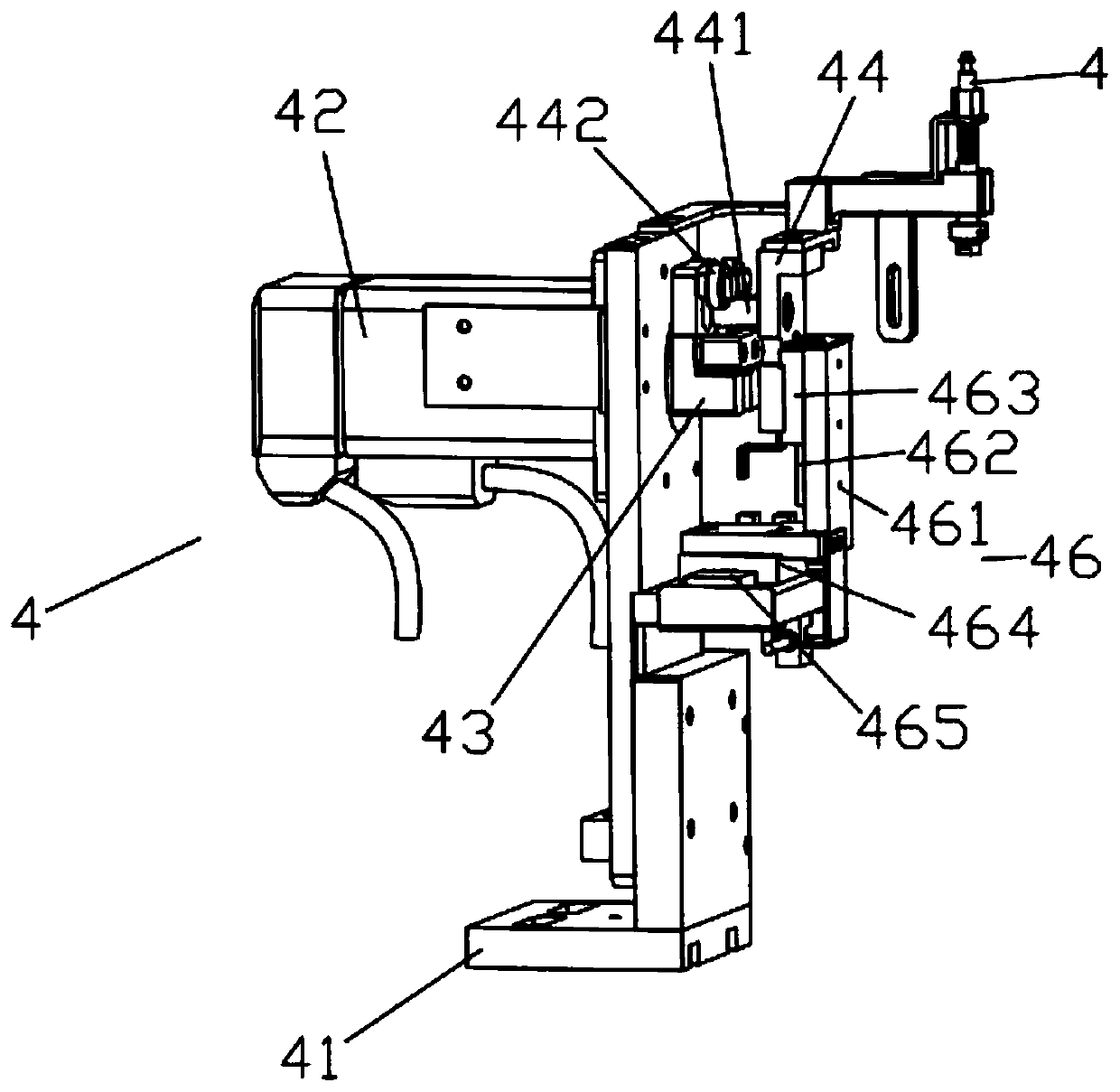
[0033] see Figure 1 to Figure 7 . It should be noted that the structures, proportions, sizes, etc. shown in the drawings attached to this specification are only used to match the content disclosed in the specification, for those who are familiar with this technology to understand and read, and are not used to limit the implementation of the present invention. Limiting conditions, so there is no technical substantive meaning, any modification of structure, change of proportional relationship or adjustment of size, without affecting the effect and purpose of the present invention, should still fall within the scope of the present invention. The disclosed technical content must be within the scope covered. At the sa...


PUM

PropertyMeasurementUnit
angleaaaaaaaaaa

Abstract

The invention provides a semiconductor detection device, and belongs to the technical field of semiconductor detection. The semiconductor detection device comprises a frame, and a control mechanism, afeeding mechanism, a material taking mechanism, a material placing mechanism, a detection mechanism and a discharging mechanism which are arranged on the frame. According to the semiconductor detection device, the control mechanism integrally controls the action of each mechanism, so that each mechanism is matched to realize the automation of semiconductor detection; the feeding mechanism automatically conveys a to-be-detected piece, the material taking mechanism takes down the to-be-detected piece from the feeding mechanism and places the to-be-detected piece on the material placing mechanism, the detection mechanism detects the to-be-detected piece on the material placing mechanism, and finally the discharging mechanism classifies, takes down and stores the to-be-detected piece according to a detection result; and the whole detection process is highly automatic, qualified products and unqualified products can be classified and collected according to detection results, and later operation is convenient.

Description

technical field [0001] The invention relates to the technical field of semiconductor detection, in particular to a semiconductor detection device. Background technique [0002] Semiconductor refers to a material whose conductivity at room temperature is between that of a conductor and an insulator. Semiconductors have a wide range of applications in radios, televisions, and temperature measurement. For example, a diode is a device made of a semiconductor. A semiconductor is a material whose electrical conductivity can be controlled, ranging from an insulator to a conductor. No matter from the perspective of technology or economic development, the importance of semiconductors is enormous. The core units of most of today's electronic products, such as computers, mobile phones or digital recorders, are closely related to semiconductors. Common semiconductor materials include silicon, germanium, gallium arsenide, etc., and silicon is the most influential one in commercial ap...

Claims


Application Information

Patent Timeline
Patent Type & Authority Applications(China)
IPC IPC(8): B07C5/02B07C5/344B07C5/36
CPCB07C5/02B07C5/344B07C5/361B07C5/362
Inventor 肖良红
Owner 苏州埃尔森自动化设备有限公司
Why Eureka
Try Eureka