A semiconductor integrated circuit device

An integrated circuit and semiconductor technology, which is applied in the field of semiconductor integrated circuit devices, can solve problems such as thinner solder pins, short circuits, and unusable equipment.

Active Publication Date: 2020-10-23
深圳市信展通电子股份有限公司
View PDF5 Cites 0 Cited by
  • Summary
  • Abstract
  • Description
  • Claims
  • Application Information

AI Technical Summary

Problems solved by technology

[0004] For this reason, the embodiment of the present invention provides a semiconductor integrated circuit device to solve the problem that in the prior art, some areas of the metal wiring layer, especially the pin connections of the device, are prone to solder pins being melted by high temperature and becoming thinner. As a result, the resistance will change, and the device will easily be broken down when the current passes through. In severe cases, the adjacent wiring layers may even melt and stick together, resulting in a short circuit in the circuit, making the device unusable.

Method used


Image

  • A semiconductor integrated circuit device
  • A semiconductor integrated circuit device
  • A semiconductor integrated circuit device

Examples


Embodiment Construction

[0035] The following specific examples illustrate the implementation of the present invention. Those familiar with this technology can easily understand the other advantages and effects of the present invention from the contents disclosed in this specification. Obviously, the described embodiments are part of the embodiments of the present invention. , Not all examples. Based on the embodiments of the present invention, all other embodiments obtained by those of ordinary skill in the art without creative work shall fall within the protection scope of the present invention.

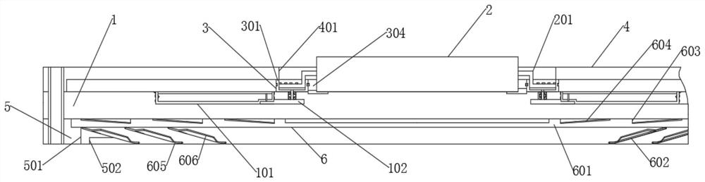
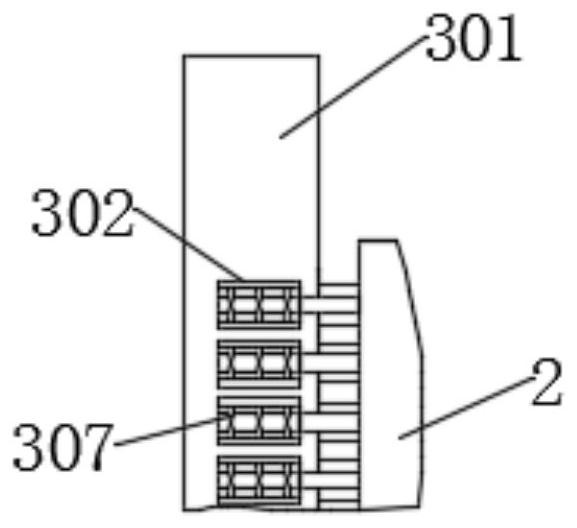
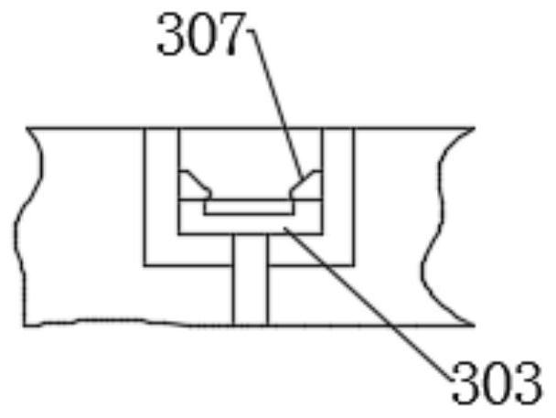
[0036] Such as figure 1 As shown, the present invention provides a semiconductor integrated circuit device, which can realize the spacing between adjacent metal wiring layers 108 and the separate isolation and welding of the device pins through the pin inserts and the storage cover 107, while The pin inserts can be freely disassembled and assembled, which is convenient for users to perform maintenance operati...


PUM


Abstract

The embodiment of the invention discloses a semiconductor integrated circuit device. The device comprises a transparent substrate, wherein a surface of one side of the transparent substrate is connected with an electric appliance element of which the side wall is provided with a plurality of pins; a pin anti-sticking mechanism connected with the pins is arranged on the surface of the transparent substrate; according to the invention, pin insertion strips and a storage cover are arranged; the interval between adjacent metal wiring layers is realized; the independent isolation welding connectionof the pins of the device is realized; meanwhile, the pin insertion strips can be freely disassembled and assembled; the maintenance operation by a user is facilitated, in the particular implementation, only the elements are clamped into similar-shaped holes, meanwhile, the pins are inserted into pin slots in a one-to-one correspondence manner; therefore, the pins can be isolated, the pins can becompletely wrapped by the pin slots after the pins are inserted into the pin slots, the normal use of the equipment is not influenced even if a partial area is thinned, and then a plurality of metalwiring layers are placed into the storage cover such that the wiring layers can be protected and spaced.

Description

Technical field [0001] The embodiment of the present invention relates to the field of semiconductors, in particular to a semiconductor integrated circuit device. Background technique [0002] Semiconductor integrated circuit refers to a semiconductor integrated circuit device with at least one circuit block on a semiconductor substrate. In its specific implementation, it combines active components such as transistors and diodes with passive components such as resistors and capacitors according to certain Circuit interconnection, "integrated" on a single semiconductor chip, to complete a specific circuit or system function. [0003] At present, the common semiconductor integrated circuit devices on the market are becoming smaller and smaller with the development of technology, and the width of the metal wiring layer used for circuit interconnection and the gap between adjacent ones are getting smaller and smaller. When the integrated circuit is in use, it A large amount of heat wi...

Claims


Application Information

Patent Timeline
Patent Type & Authority Patents(China)
IPC IPC(8): H01L23/48H01L23/488H01L23/367
CPCH01L23/367H01L23/48H01L23/488
Inventor 施锦源周建海
Owner 深圳市信展通电子股份有限公司
Why Eureka
Try Eureka