Electric power conversion device
A technology for power conversion devices and power terminals, which is applied to circuits, electrical components, and electrical solid devices, to achieve cooling performance and productivity improvements, reduce manufacturing man-hours, and improve productivity
- Summary
- Abstract
- Description
- Claims
- Application Information
AI Technical Summary
Problems solved by technology
Method used
Image
Examples
Embodiment approach 1
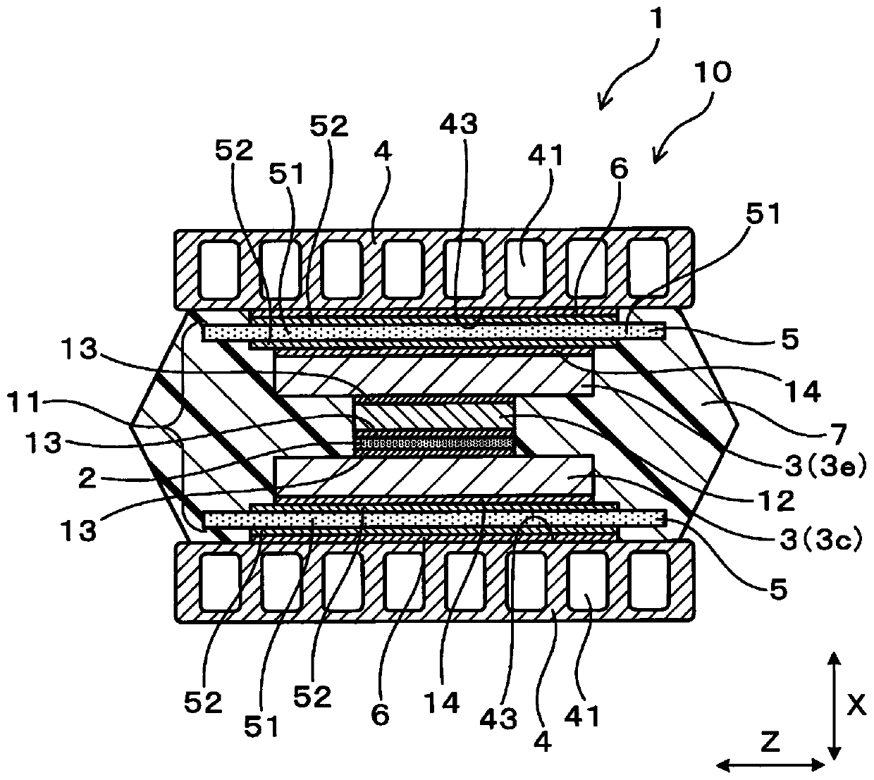
[0059] refer to Figure 1 to Figure 12 Embodiments of the power conversion device will be described.
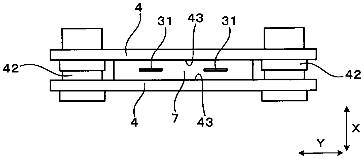
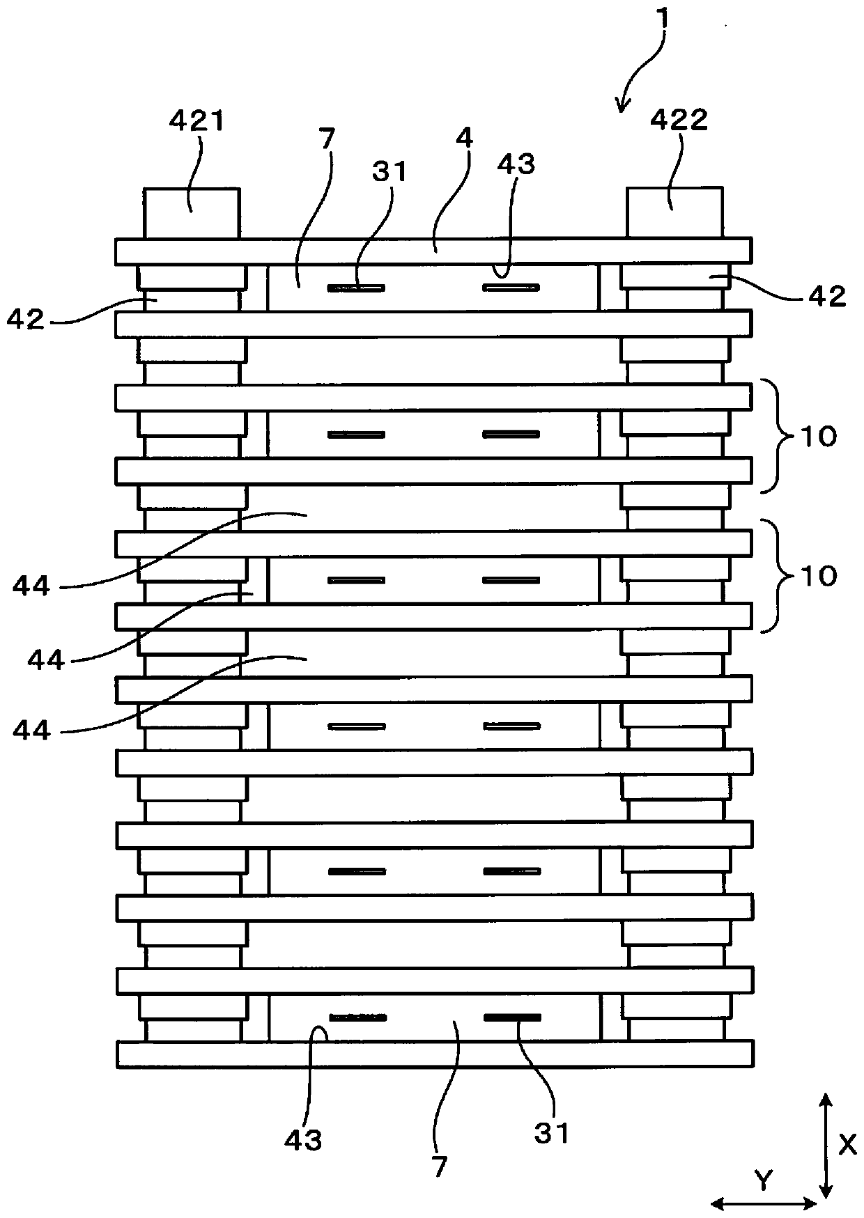
[0060] Such as figure 1 As shown, the power conversion device 1 of the present embodiment has a semiconductor element 2 , a plurality of lead frames 3 , a cooling pipe 4 , an insulating portion 5 , a metal bonding material 6 , and a resin sealing portion 7 .
[0061] The lead frame 3 is electrically connected to the semiconductor element 2 . The cooling pipe 4 is one form of a channel forming body in which a refrigerant channel 41 through which the refrigerant flows is formed. The insulating part 5 is arranged between the lead frame 3 and the cooling pipe 4 to insulate them. Metal joint material 6 joins insulating portion 5 and cooling pipe 4 . The resin sealing portion 7 seals the semiconductor element 2 and the lead frame 3 .
[0062] The resin sealing portion 7 integrates the semiconductor element 2 and the lead frame 3 with the cooling pipe 4 to form a semiconductor ...
Embodiment approach 2
[0098] In the power conversion device 1 of the present embodiment, if Figure 13 As shown, the semiconductor cooling unit 10 has a plurality of semiconductor components 2 . That is, one semiconductor cooling module 10 has a plurality of semiconductor elements 2 arranged side by side in a direction perpendicular to the stacking direction X between a pair of cooling pipes 4 . also, Figure 13 is a cross-sectional view of the semiconductor cooling module 10 on a plane perpendicular to the longitudinal direction Z.
[0099] In this embodiment, a plurality of semiconductor elements 2 are arranged side by side in the lateral direction Y.
[0100] In addition, at least two of the plurality of semiconductor elements 2 in the semiconductor cooling unit 10 are an upper arm semiconductor element 2u and a lower arm semiconductor element 2d connected in series to each other. In addition, in this embodiment, the number of semiconductor elements 2 built in the semiconductor cooling unit 1...
Embodiment approach 3
[0117] Such as Figure 18 ~ Figure 20 As shown, the power conversion device 1 of the present embodiment has a configuration in which the insulating portion 5 is arranged over the two laminated component groups 11 .
[0118] That is, if Figure 18 As shown, two laminated component groups 11 share two insulating portions 5 . One insulating portion 5 is bonded to an opposing surface 43 of one cooling pipe 4 via a metal bonding material 6 . In addition, one insulating portion 5 is bonded to the opposing surface 43 of the other cooling pipe 4 via the metal bonding material 6 . Further, two semiconductor elements 2 are arranged side by side together with the lead frame 3 and the terminal chip 12 between the pair of insulating portions 5 arranged to face each other in the stacking direction X. As shown in FIG.
[0119] In addition, in this embodiment, if Figure 18 , Figure 19 As shown, on one main surface of the insulating portion 5, two metal layers 52 are formed at two posit...
PUM
 Abstract
Description
Claims
Application Information
 - R&D Engineer
- R&D Manager
- IP Professional
- Industry Leading Data Capabilities
- Powerful AI technology
- Patent DNA Extraction
Browse by: Latest US Patents, China's latest patents, Technical Efficacy Thesaurus, Application Domain, Technology Topic, Popular Technical Reports.
© 2024 PatSnap. All rights reserved.Legal|Privacy policy|Modern Slavery Act Transparency Statement|Sitemap|About US| Contact US: help@patsnap.com


