A quantum dot light emitting diode
A quantum dot light-emitting and diode technology, applied in the field of quantum dots, can solve the problems of unbalanced carrier injection, affecting the luminous efficiency and life of the device, and reducing the probability of carrier recombination, so as to improve the recombination efficiency, balance the injection rate, Effect of improving luminous efficiency
- Summary
- Abstract
- Description
- Claims
- Application Information
AI Technical Summary
Problems solved by technology
Method used
Image
Examples
preparation example Construction
[0035] Such as image 3 As shown, some embodiments of the present invention also provide a method for preparing a seed-dot light-emitting diode, comprising the following steps:
[0036] S01 provides the substrate;
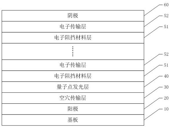
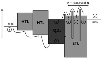
[0037] S03 Form a functional layer on the substrate, the functional layer includes n layers of stacked functional structural units, the functional structural units are composed of stacked electron blocking material layers and electron transport layers, and in the functional structural units The electron blocking material layer is set close to the quantum dot light-emitting layer, the electron transport layer in the functional structural unit is set close to the cathode, and the n is an integer greater than or equal to 2.
[0038] Specifically, quantum dot light-emitting diodes are divided into upright structures and inverted structures. The upright structure includes a stacked anode, a cathode, and a quantum dot light-emitting layer arranged between the anode and...
Embodiment 1
[0051] A quantum dot light-emitting diode, which includes a stacked substrate, an anode, a hole injection layer, a hole transport layer, a quantum dot light-emitting layer, a functional layer, and a cathode from bottom to top, and the functional layer includes 5 alternately stacked layers. A layer of electron blocking material layer and 5 layers of electron transport layers, the bottom layer of the functional layer is an electron blocking material layer and is arranged close to the quantum dot light-emitting layer, and the top layer of the functional layer is an electron transport layer and is arranged near the cathode; along the anode To the direction of the cathode, the material of each electron blocking material layer is PVK, PVK doped with 1.5wt.%Li-TFSI, PVK doped with 3wt.%Li-TFSI, 4.5wt.%Li- The PVK of TFSI and the PVK of 6wt.%Li-TFSI; The anode is ITO, and the thickness is 100nm; The hole injection layer material is PEDOT:PSS, and the thickness is 40 nm; The hole transp...
Embodiment 2
[0053] A quantum dot light-emitting diode, which includes a stacked substrate, an anode, a hole injection layer, a hole transport layer, a quantum dot light-emitting layer, a functional layer, and a cathode from bottom to top, and the functional layer includes 5 alternately stacked layers. A layer of electron blocking material layer and 5 layers of electron transport layers, the bottom layer of the functional layer is an electron blocking material layer and is arranged close to the quantum dot light-emitting layer, and the top layer of the functional layer is an electron transport layer and is arranged near the cathode; along the anode To the direction of the cathode, the material of each electron blocking material layer is TFB, TFB doped with 1.5wt.%Li-TFSI, TFB doped with 3wt.%Li-TFSI, 4.5wt.%Li- The TFB of TFSI and the TFB of 6wt.%Li-TFSI; The anode is ITO, and the thickness is 100nm; The hole injection layer material is PEDOT:PSS, and the thickness is 40 nm; The hole transp...
PUM
| Property | Measurement | Unit |
|---|---|---|
| thickness | aaaaa | aaaaa |
| thickness | aaaaa | aaaaa |
| thickness | aaaaa | aaaaa |
Abstract
Description
Claims
Application Information


