Forming method of semiconductor device
A semiconductor and device technology, which is applied in the field of semiconductor device formation, can solve the problems such as difficult to keep the height of metal gate consistent, and the electrical performance of the device is reduced, so as to achieve the effect of improving electrical performance and accurate height and dimension
- Summary
- Abstract
- Description
- Claims
- Application Information
AI Technical Summary
Problems solved by technology
Method used
Image


Examples
Embodiment Construction
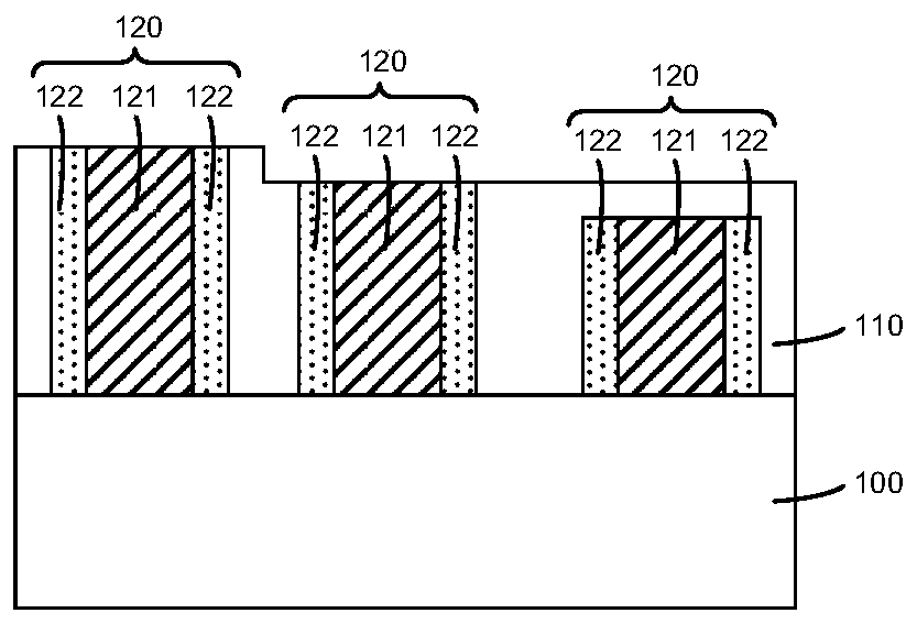
[0024] As mentioned above, there is a problem that the top surface of the remaining gate structure is uneven when adjusting the height of the gate structure in the existing technology.
[0025] After research, it is found that the reason for the above problems is that the material of the gate is different from that of the high-k dielectric layer or the work function layer. Therefore, after the subsequent direct etching of the gate structure, the etching process has a negative effect on the gate and the high-k dielectric layer. The etch rate of the dielectric layer or the work function layer is different, resulting in an uneven top of the final gate structure.
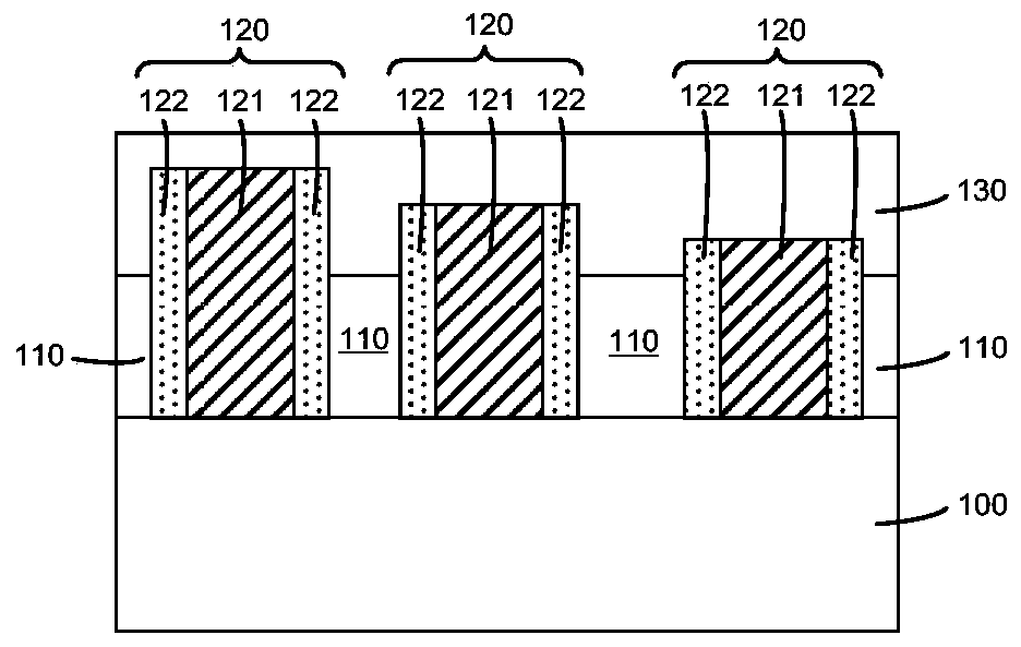
[0026] In order to solve this problem, the present invention provides a method for forming a semiconductor device. Before etching the gate structure, an interlayer dielectric layer with a uniform material is etched to make the remaining interlayer dielectric layer have a certain height. This height is also The final hei...
PUM
| Property | Measurement | Unit |
|---|---|---|
| Depth | aaaaa | aaaaa |
Abstract
Description
Claims
Application Information