

Totem pole circuit
A totem pole and circuit technology, applied to logic circuits, electrical components, improved amplifiers to reduce temperature/power supply voltage changes, etc., can solve problems such as unstable waveforms, complex drive circuits, and different temperature characteristics of NPN triodes, etc., to achieve The effect of output waveform stabilization
- Summary
- Abstract
- Description
- Claims
- Application Information
AI Technical Summary
Problems solved by technology
Method used
Image

Examples
Embodiment Construction
[0022] Below, the present invention will be further described in conjunction with the accompanying drawings and specific implementation methods. It should be noted that, under the premise of not conflicting, the various embodiments described below or the technical features can be combined arbitrarily to form new embodiments. .
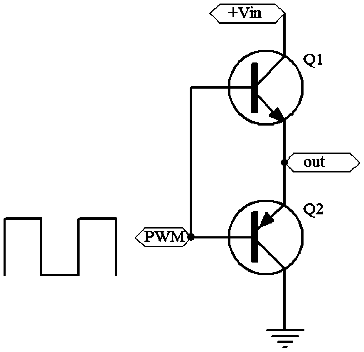
[0023] A totem pole circuit has a stable totem pole output, and at the same time, the circuit has a reverse output function, which simplifies the driving circuit.
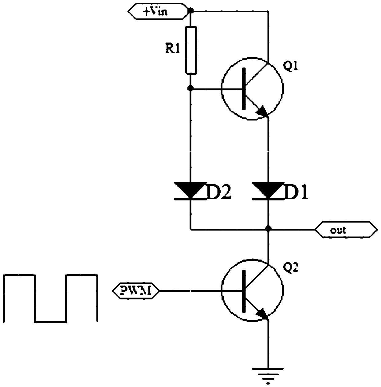
[0024] refer to image 3 As shown, the totem pole circuit includes two NPN transistors with the same characteristics, named NPN transistor Q1 and NPN transistor Q2 respectively; secondly, the totem pole circuit also includes two diodes D1 and D2.
[0025] The collector of the NPN transistor Q1 is connected to the input voltage Vin, the input voltage Vin is connected to the base of the NPN transistor Q1 through the resistor R1, the emitter of the NPN transistor Q1 is connected to the anode ...
PUM
 Abstract
Description
Claims
Application Information