Supercharge Your Innovation With Domain-Expert AI Agents!

PCB image block sampling device and method based on correlation analysis

A technology of correlation analysis and image segmentation, applied in image analysis, image enhancement, image data processing and other directions, can solve the problem of wasting computing power, and achieve the effect of reducing the amount of calculation, improving the detection speed and detection accuracy

Active Publication Date: 2020-07-14
TSINGHUA UNIV
View PDF4 Cites 1 Cited by
  • Summary
  • Abstract
  • Description
  • Claims
  • Application Information

AI Technical Summary

Problems solved by technology

These two methods need to detect a large number of hollow areas and PCB areas equally in the middle, wasting a lot of computing power

Method used


Image

  • PCB image block sampling device and method based on correlation analysis
  • PCB image block sampling device and method based on correlation analysis
  • PCB image block sampling device and method based on correlation analysis

Examples


Embodiment Construction

[0040] Embodiments of the present invention are described in detail below, examples of which are shown in the drawings, wherein the same or similar reference numerals designate the same or similar elements or elements having the same or similar functions throughout. The embodiments described below by referring to the figures are exemplary and are intended to explain the present invention and should not be construed as limiting the present invention.

[0041] The PCB image block sampling device and method based on correlation analysis according to the embodiments of the present invention will be described below with reference to the accompanying drawings. First, the PCB image block sampling device based on correlation analysis according to the embodiments of the present invention will be described with reference to the accompanying drawings.

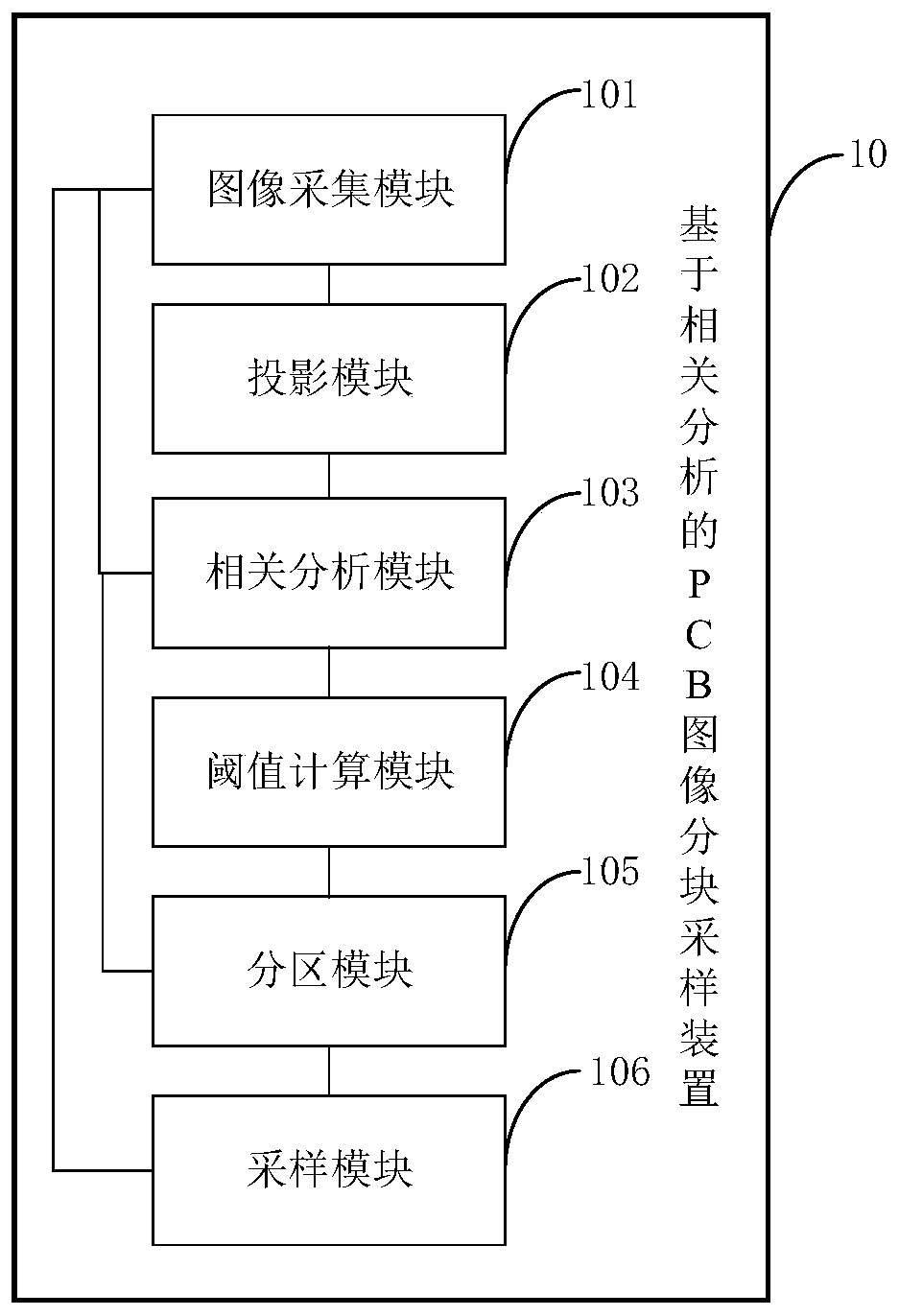
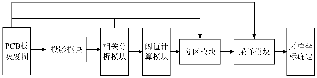
[0042] figure 1 It is a structural schematic diagram of a PCB image block sampling device based on correlation analysis according to an ...


PUM


Abstract

The invention discloses a PCB image block sampling device and method based on correlation analysis, and the device mainly comprises a projection module, a correlation analysis module, a threshold calculation module, and a partitioning module. The projection module is used for projecting the grayscale image to a two-dimensional coordinate system to generate a projection array; the correlation analysis module is used for performing data correlation analysis on the projection array to generate an autocorrelation coefficient sequence; the threshold calculation module is used for calculating the autocorrelation coefficient sequence by using a correlation threshold algorithm to obtain a partition division threshold; the partitioning module is used for processing the PCB grayscale image by utilizing the autocorrelation coefficient sequence and a partitioning threshold value to generate a regional coordinate list of the PCB daughter board; and the sampling module is used for performing image block sampling on the PCB grayscale image according to the regional coordinate list of the PCB daughter board, and determining the coordinates of a sampling frame. The device reduces the calculation amount, improves the detection speed and detection precision of PCB defects, and can be suitable for partitioning and sampling other images.

Description

technical field [0001] The invention relates to the technical field of computer software engineering, in particular to a PCB image block sampling device and method based on correlation analysis. Background technique [0002] When using a convolutional neural network to detect defects on a PCB (Printed Circuit Board, printed circuit board), it is usually necessary to load the image of the PCB to be detected into a GPU (Graphics Processing Unit, graphics processor), and then use CNN (Convolutional Neural Networks, Convolutional Neural Networks) for inference. However, in the actual production process, due to the consideration of technological process and efficiency, each complete PCB board on the assembly line includes several identical small PCB boards. The image obtained by the camera is about 100 million pixels, which is very large. Due to capacity limitations, such a large image cannot be loaded into the GPU for detection at one time, so it is necessary to find a suitabl...

Claims


Application Information

Patent Timeline
IPC IPC(8): G06T7/00G06T7/136G06T7/11G06T7/73
CPCG06T7/0004G06T7/136G06T7/11G06T7/73G06T2207/30141
Inventor 罗贵明何悦
Owner TSINGHUA UNIV
Features
  • R&D
  • Intellectual Property
  • Life Sciences
  • Materials
  • Tech Scout
  • Unparalleled Data Quality
  • Higher Quality Content
  • 60% Fewer Hallucinations
Learn More