Wafer positioning calibration device and wafer positioning calibration method

A technology of calibration device and calibration method, which is applied in the direction of electrical components, semiconductor/solid-state device manufacturing, circuits, etc., can solve problems that affect the precision and efficiency of semiconductor processes, unstable reliability of mechanical devices, and precision deviation, etc., to achieve digitalization Management and detection, realizing early warning of position deviation, and reducing the effect of calibration time

Active Publication Date: 2020-07-17
SHANGHAI GUONA SEMICON TECH CO LTD
View PDF6 Cites 7 Cited by
  • Summary
  • Abstract
  • Description
  • Claims
  • Application Information

AI Technical Summary

Problems solved by technology

However, due to the problem of the structure of the notch mark itself, there is a huge deviation in the accuracy of the position determination of the notch mark, and the turntable must rotate one or more times in the process of obtaining the wafer notch, the efficiency is low, and the reliability of the mechanical device is also not good. Stability factor, so the working performance of the wafer alignment device directly affects the accuracy and efficiency of the semiconductor process

Method used


Image

  • Wafer positioning calibration device and wafer positioning calibration method
  • Wafer positioning calibration device and wafer positioning calibration method
  • Wafer positioning calibration device and wafer positioning calibration method

Examples


Embodiment Construction

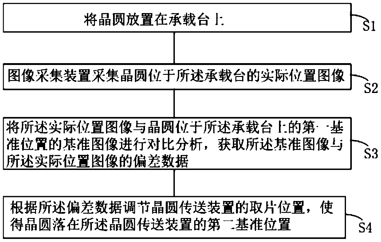
[0027] A wafer positioning calibration device proposed by the present invention will be further described in detail below in conjunction with the accompanying drawings and specific embodiments.

[0028] The wafer alignment calibration device 100 according to an embodiment of the present invention will be described below with reference to the accompanying drawings.

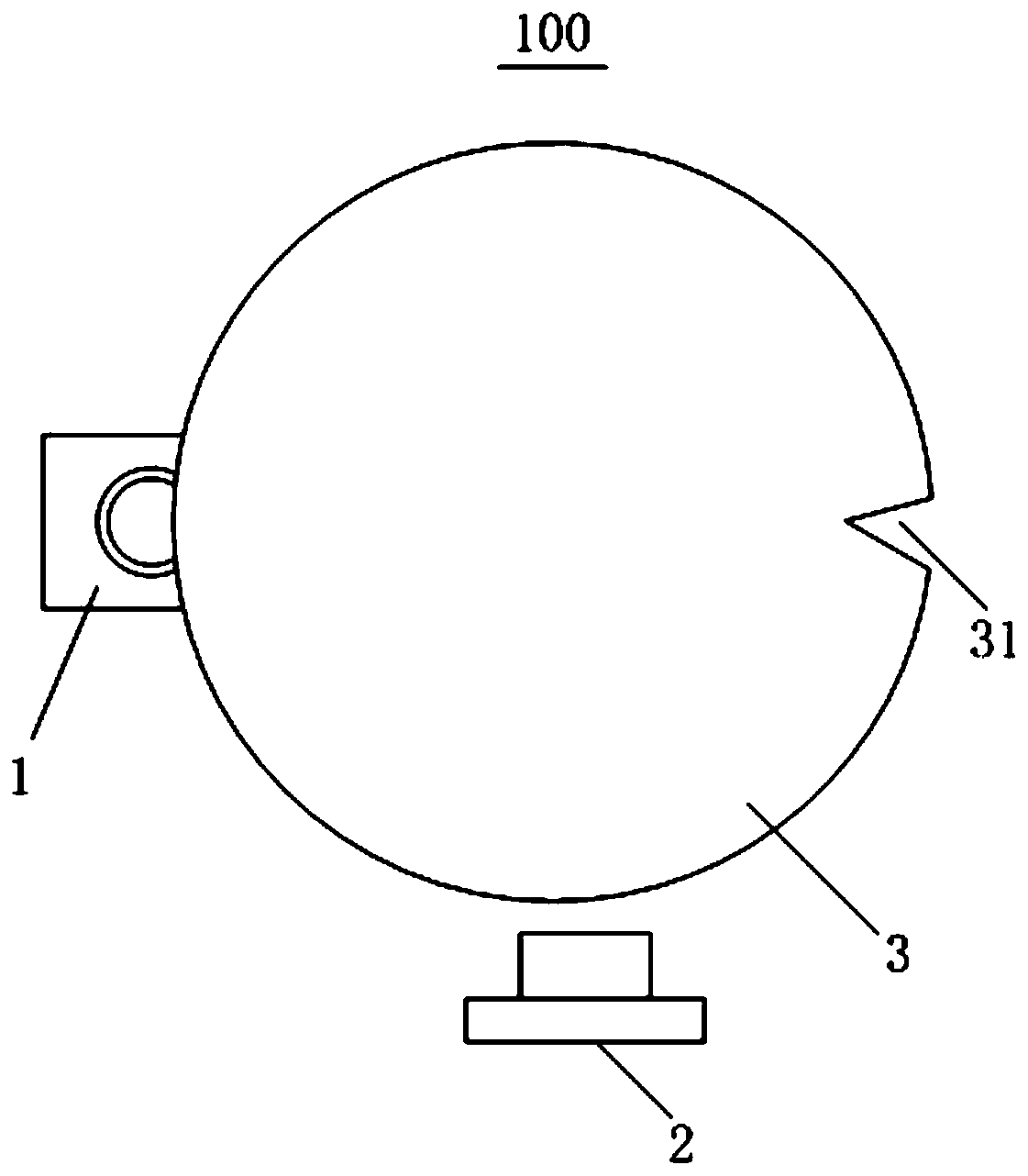
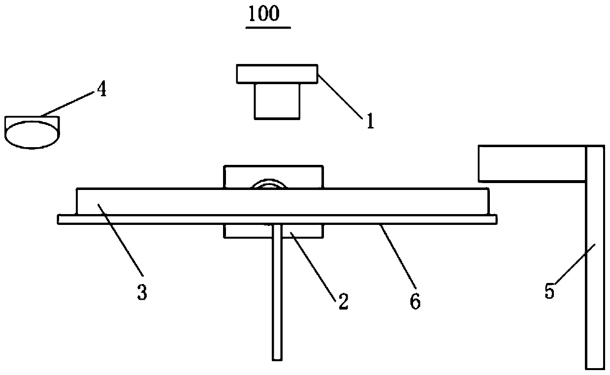
[0029] Such as figure 1 with figure 2 As shown, the wafer positioning calibration device 100 according to the embodiment of the present invention may include a carrier table 6, an image acquisition device (such as figure 1 with figure 2 The first image acquisition device 1 and the second image acquisition device 2) and the wafer transfer device 5 and the control device are shown.

[0030] The carrier table 6 is used to carry the wafer 3. The carrier table 6 is provided with a first reference positioning position for placing the wafer 3. When the wafer 3 is placed at the first reference position, it can be ensu...


PUM


Abstract

The invention discloses a wafer positioning calibration device and a wafer positioning calibration method, the wafer positioning calibration device comprises a bearing table, an image acquisition device, a wafer conveying device and a control device, and the image acquisition device is used for acquiring an actual position image of a wafer on the bearing table; the control device is connected withthe image acquisition device and the wafer conveying device; a reference image of the wafer at the first reference position is stored in the control device; and the control device acquires the actualposition image acquired by the image acquisition device, compares and analyzes the actual position image and the reference image to acquire deviation data of the actual position and the reference image, and adjusts the mechanical arm according to the deviation data to enable the wafer to fall at the second reference position. According to the embodiment of the invention, the wafer positioning calibration device has the advantages of simple structure, good stability, low energy consumption, high speed, accuracy, systematic data management and the like.

Description

technical field [0001] The invention relates to the field of semiconductor equipment, in particular to a wafer positioning calibration device and a wafer positioning calibration method. Background technique [0002] The semiconductor processing process involves a variety of processes, and each process requires different equipment. Many processes need to obtain the accurate position of the wafer in advance. In the prior art, the wafer alignment device, which is one of the key parts of semiconductor equipment Generally, an optical sensor system (light source + photosensitive sensor) is used to cooperate with the rotation of the turntable to obtain notch information on the edge of the wafer to achieve wafer alignment. However, due to the problem of the structure of the notch mark itself, there is a huge deviation in the accuracy of the position determination of the notch mark, and the turntable must rotate one or more times in the process of obtaining the wafer notch, the effic...

Claims


Application Information

Patent Timeline
Patent Type & Authority Applications(China)
IPC IPC(8): H01L21/68
CPCH01L21/681Y02P70/50
Inventor 毕迪
Owner SHANGHAI GUONA SEMICON TECH CO LTD
Why Eureka
Try Eureka