Display substrate, preparation method thereof and display device

A technology for display substrates and substrate substrates, applied in semiconductor/solid-state device manufacturing, semiconductor devices, electrical components, etc. Improve brightness uniformity, avoid time consumption, and achieve uniform film thickness

Active Publication Date: 2020-07-28
BOE TECH GRP CO LTD
View PDF5 Cites 5 Cited by
  • Summary
  • Abstract
  • Description
  • Claims
  • Application Information

AI Technical Summary

Problems solved by technology

However, the error in the amount of ink ejected between multiple nozzles will lead to non-uniform film thickness between sub-pixels, resulting in differences in brightness uniformity between pixels

Method used


Image

  • Display substrate, preparation method thereof and display device
  • Display substrate, preparation method thereof and display device
  • Display substrate, preparation method thereof and display device

Examples


preparation example Construction

[0086] The embodiment of the present invention also provides a method for preparing a display substrate, the method comprising:

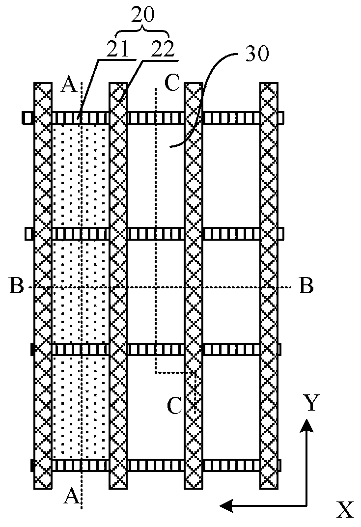
[0087] S1: forming a pixel defining layer on one side of the base substrate, the pixel defining layer defines a plurality of sub-pixel regions;

[0088] S2: Inkjet printing hole injection ink on the side of the pixel defining layer away from the base substrate, and the hole injection inks of at least two adjacent sub-pixel regions are connected.

[0089] In an exemplary embodiment, S1 may include:

[0090] A wall layer extending along a first direction and a second pixel wall extending along a second direction are formed on one side of the base substrate, the wall layer and the second pixel wall intersect to define the In the sub-pixel area, the height of the partition wall layer is smaller than the height of the second pixel partition wall, the first direction and the second direction are perpendicular to each other, and the size of the sub-pixel ...


PUM

PropertyMeasurementUnit
heightaaaaaaaaaa
heightaaaaaaaaaa
critical temperatureaaaaaaaaaa

Abstract

The invention discloses a display substrate, a preparation method thereof and a display device. The display substrate comprises an underlayer substrate, a pixel defining layer and a light-emitting structure layer, wherein the pixel defining layer is arranged on one side of the underlayer substrate, and a plurality of sub-pixel areas are defined by the pixel defining layer; and the light-emitting structure layer is arranged on the side, which is away from the underlayer substrate, of the pixel defining layer and located in the sub-pixel areas, the light-emitting structure layer comprises a holeinjection layer, and when hole injection ink is formed in the sub-pixel areas through an ink-jet printing method, the hole injection ink of at least two adjacent sub-pixel areas is communicated. According to the display substrate, the film thicknesses of the hole injection layers of at least two adjacent sub-pixel areas can be uniform, the film thickness difference between sub-pixels is reduced,and the brightness uniformity between the pixels is improved.

Description

technical field [0001] The invention relates to the field of display technology, in particular to a display substrate, a preparation method thereof, and a display device. Background technique [0002] Organic Light Emitting Diode (English: Organic Light Emitting Diode, referred to as OLED) display substrate is widely used in mobile phones, tablet computers, digital cameras, etc. due to its advantages of low energy consumption, low production cost, self-illumination, wide viewing angle and fast response speed. field. [0003] Currently, OLED devices can be formed by inkjet printing. However, the error in the amount of ink ejected between multiple nozzles will lead to non-uniform film thickness among sub-pixels, resulting in differences in brightness uniformity among pixels. Contents of the invention [0004] The purpose of the embodiments of the present invention is to provide a display substrate to improve the uniformity of film thickness of sub-pixels. [0005] In orde...

Claims


Application Information

Patent Timeline
Patent Type & Authority Applications(China)
IPC IPC(8): H01L51/50H01L51/56H01L27/32H01L21/77
CPCH10K59/35H10K59/122H10K59/12H10K71/135H10K50/17H10K59/1201Y02E10/549
Inventor 崔颖侯文军
Owner BOE TECH GRP CO LTD
Why Eureka
Try Eureka