Universal quantum walk analog chip structure based on integrated optics

An analog chip and integrated optics technology, which is applied in the field of quantum computing and integrated optics, can solve the problems of limited control of elements and difficulty in meeting the application requirements of practical quantum walk calculations.

Active Publication Date: 2020-07-31
NAT UNIV OF DEFENSE TECH
View PDF2 Cites 8 Cited by
  • Summary
  • Abstract
  • Description
  • Claims
  • Application Information

AI Technical Summary

Problems solved by technology

However, most of these demonstrations can only perform the quantum walk evolution of a specific Hamiltonian, and the control of many elements in the evolution process is relatively limited, which is difficult to meet the application requirements of practical quantum walk calculations.

Method used


Image

  • Universal quantum walk analog chip structure based on integrated optics
  • Universal quantum walk analog chip structure based on integrated optics
  • Universal quantum walk analog chip structure based on integrated optics

Examples


example 1

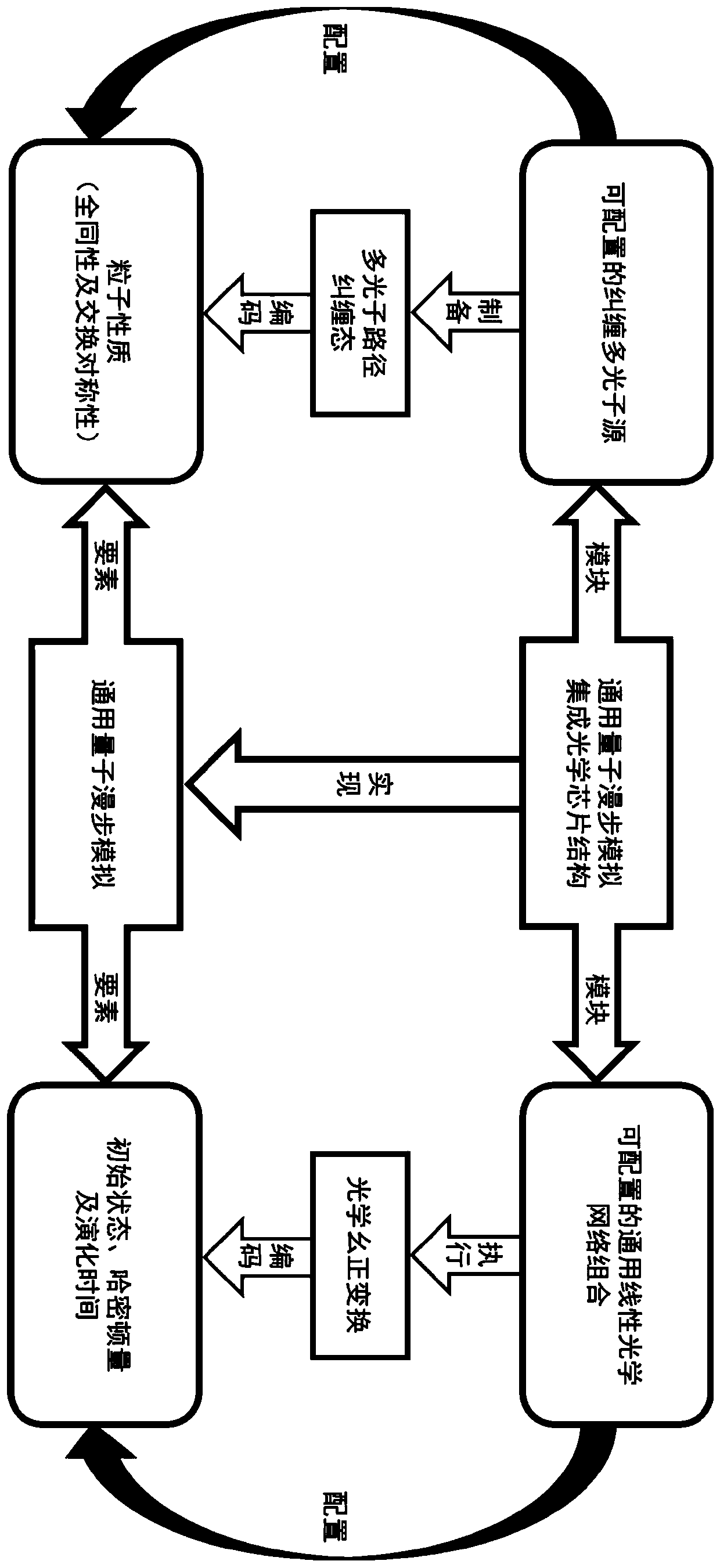
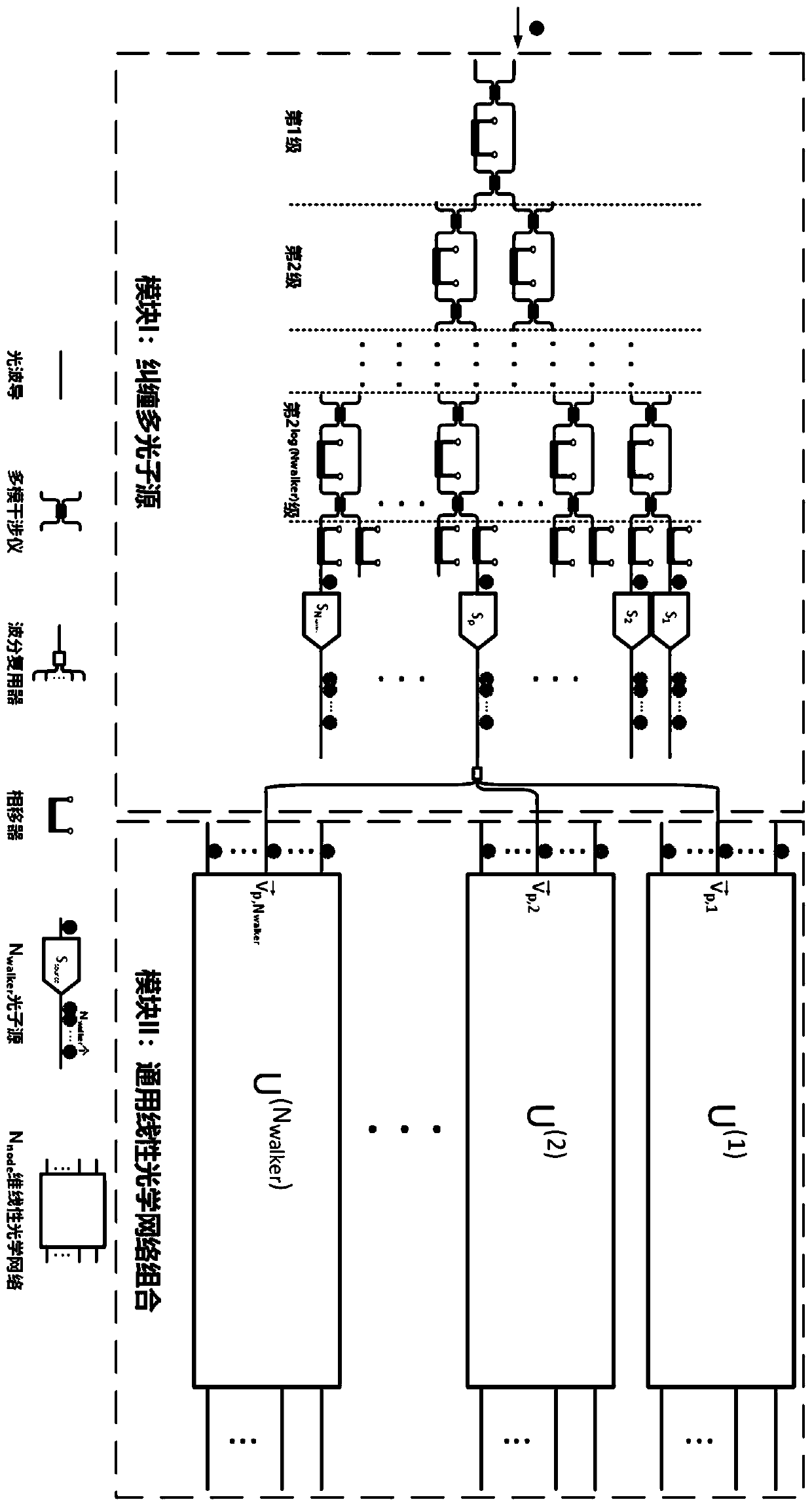
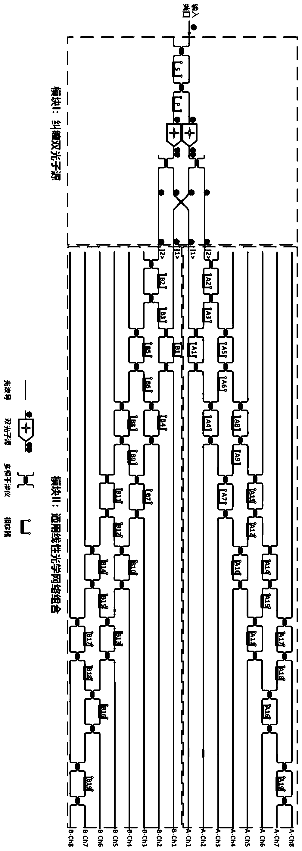
[0028] The general quantum walk of two quantum particles starting from nodes 1 and 2 on the 8-node graph G simulates the optical chip structure, such as image 3 As shown, the chip structure is composed of two modules, the first half is the configurable entangled multi-photon source module I: entangled two-photon source, and the second half is the general linear optical network combination module II: two 8-dimensional general linear optical networks A and B, each optical network structure can realize the universal linear optical unitary transformation with fixed input ports (here 1, 2). The whole chip structure is controlled by 40 phase shifters. Using this chip structure to simulate indistinguishability γ, exchange symmetry φ, walk time t, walk Hamiltonian H G The two particles start from nodes 1 and 2, and when the distribution results after the quantum walk, the chip structure needs to be configured and operated as follows:

[0029] 1. Configure the 2 phase shifters S and...


PUM


Abstract

The invention discloses a universal quantum walk analog chip structure based on integrated optics. A multi-photon source capable of preparing a multi-photon path entangled state and a linear optical network capable of achieving unitary transformation are organically combined and used in cooperation, and the corresponding relation among the on-chip multi-photon path entangled state, the unitary transformation, the quantum walking state of multi-particle quantum walking and the walking process is established. Optical unitary transformation is realized by regulating and controlling a multi-photonpath entangled state prepared by a multi-photon source and a universal linear optical network; the chip structure can carry out general quantum walk simulation with configurable elements such as evolution Hamiltonian quantity, evolution time, initial evolution state, particle properties (such as particle isotropy and particle exchange symmetry) and the like of multi-particle quantum walk.

Description

technical field [0001] The invention relates to a universal quantum walk simulation chip structure applicable to various waveguide materials by using quantum computing theory and integrated optical technology, capable of performing evolution Hamiltonian, evolution time, initial evolution state and particle properties of multi-particle quantum walk (such as particle identity, particle exchange symmetry) and other elements can be configured general quantum walk simulation, belongs to the field of quantum computing and integrated optics. Background technique [0002] Quantum Walk (Quantum Walk) is a quantized version of the classical Random Walk (Random Walk) model, which is used to describe the physical process of particles with quantum properties randomly walking in a discretized space. Such a discretized space can usually be represented by a graph composed of points and lines in mathematics, and the adjacency matrix of the graph gives the Hamiltonian for the evolution of the...

Claims


Application Information

Patent Timeline
Patent Type & Authority Applications(China)
IPC IPC(8): H04B10/70H04L9/08
CPCH04B10/70H04L9/0852H04L9/0858G02F1/212G06N10/60G06N10/40G06N10/00G01J1/44G01J2001/442
Inventor 强晓刚吴俊杰王易之
Owner NAT UNIV OF DEFENSE TECH
Why Eureka
Try Eureka