Wafer transmission device, wafer transmission method and CMP equipment cleaning module

A technology of a transmission device and a transmission method, which is applied in the directions of transportation and packaging, conveyor objects, electrical components, etc., can solve the problems of wafer cleaning effect, drop, etc., and achieve shortened transmission time, high cleanliness, and reduced handling. effect of time

Inactive Publication Date: 2020-08-11
HANGZHOU ZHONGGUI ELECTRONICS TECH CO LTD
View PDF11 Cites 2 Cited by
  • Summary
  • Abstract
  • Description
  • Claims
  • Application Information

AI Technical Summary

Problems solved by technology

Among them, there will be several units for cleaning the wafer in the cleaning system, and the wafer needs to be cleaned through each unit in turn. In this process, a device for moving the wafer is required to complete the task of moving the wafer. The claw clamping arm puts the wafers to be cleaned into the cleaning module, and takes out the cleaned wafers from the unit. The entire device needs to be kept highly clean. The existing devices use the transmission device to be installed in a suspended manner, but During use, the device will cause impurities and particles on the device to fall into the cleaning module due to wear and friction, which will affect the effect of wafer cleaning

Method used


Image

  • Wafer transmission device, wafer transmission method and CMP equipment cleaning module
  • Wafer transmission device, wafer transmission method and CMP equipment cleaning module
  • Wafer transmission device, wafer transmission method and CMP equipment cleaning module

Examples


Embodiment 1

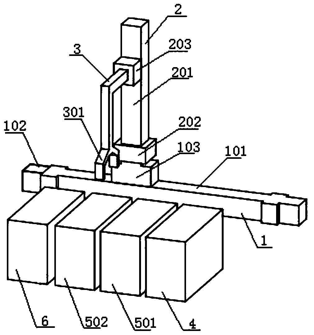
[0046] Such as figure 1 As shown, it is the first embodiment of a cleaning module of CMP equipment provided by the present invention. The wafer transfer device of the cleaning module of CMP equipment includes an X-axis moving module 1, a Z-axis moving module 2 and a clamping jaw Arm module 3; the X-axis moving module 1 is located on one side of the CMP equipment cleaning module, and the X-axis moving module includes an X transmission shaft 101, an X-axis driver 102, and an X-axis moving slider 103; the Z-axis moving Module 2 is fixedly installed on the X-axis moving slider 103, and the Z-axis moving module 2 includes a Z transmission shaft 201, a Z-axis driver 202, and a Z-axis moving slider 203; the jaw clamping arm module 3 is installed On the Z-axis moving slider 203 , the jaw clamping arm module 3 includes a jaw clamping arm 301 , which can rotate around the Z-axis moving slider 203 .

[0047] The wafer transfer method of the wafer transfer device of this embodiment is: ...

Embodiment 2

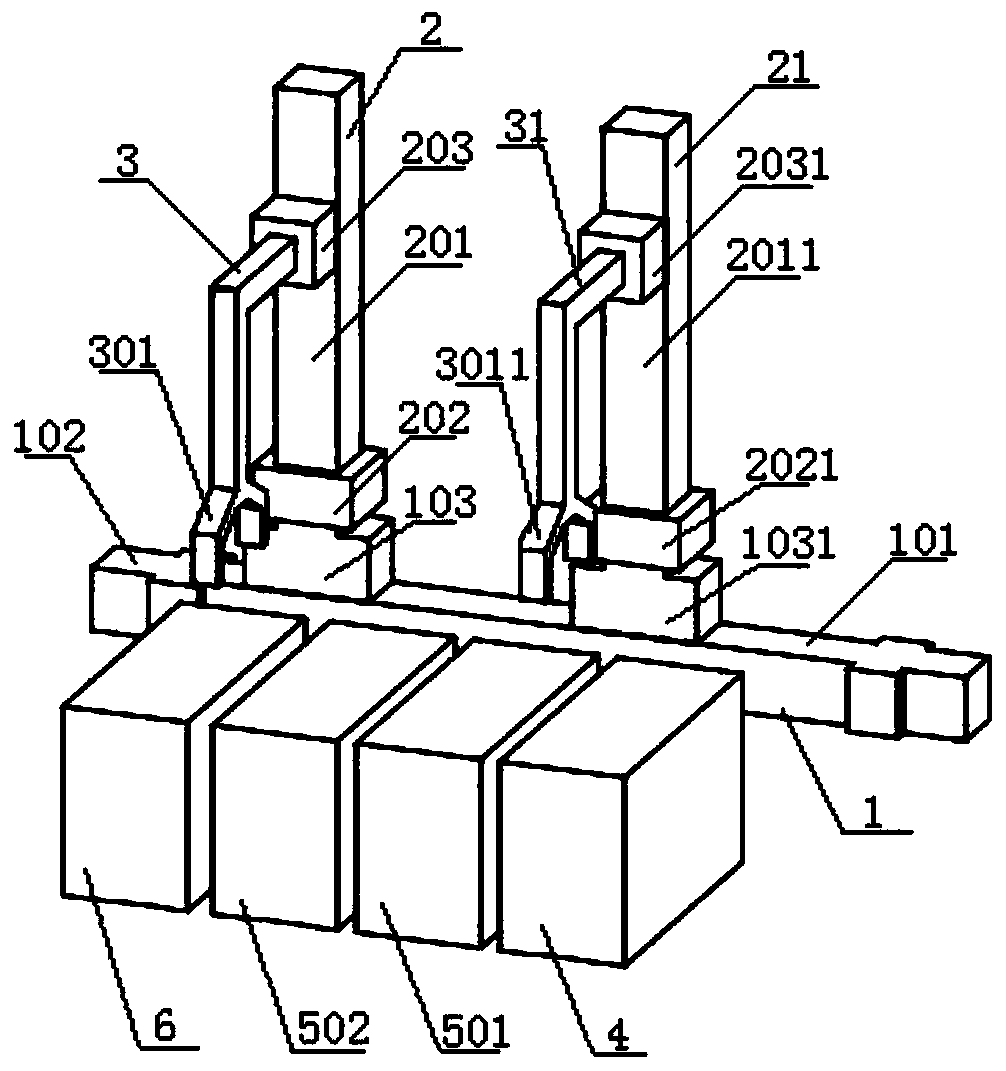
[0050] Such as figure 2 Shown is the second embodiment of a CMP equipment cleaning module provided by the present invention. Compared with the first embodiment, the second embodiment includes a first Z-axis moving module 21 and a first The jaws grip the arm module 31 . The wafer transfer device of the CMP equipment cleaning module provided in this embodiment includes an X-axis moving module 1, a Z-axis moving module 2, a first Z-axis moving module 21, a jaw clamping arm module 3 and a first jaw clamping arm Module 31; the X-axis moving module 1 is located on one side of the CMP equipment cleaning module, and the X-axis moving module includes an X transmission shaft 101, an X-axis driver 102, an X-axis moving slider 103, and a first X-axis moving slider 1031 , the X-axis moving slider 103 and the first X-axis moving slider 1031 move independently on the X transmission shaft 101; the Z-axis moving module 2 is fixedly mounted on the X-axis moving slider 103, and the Z-axis movi...

Embodiment 3

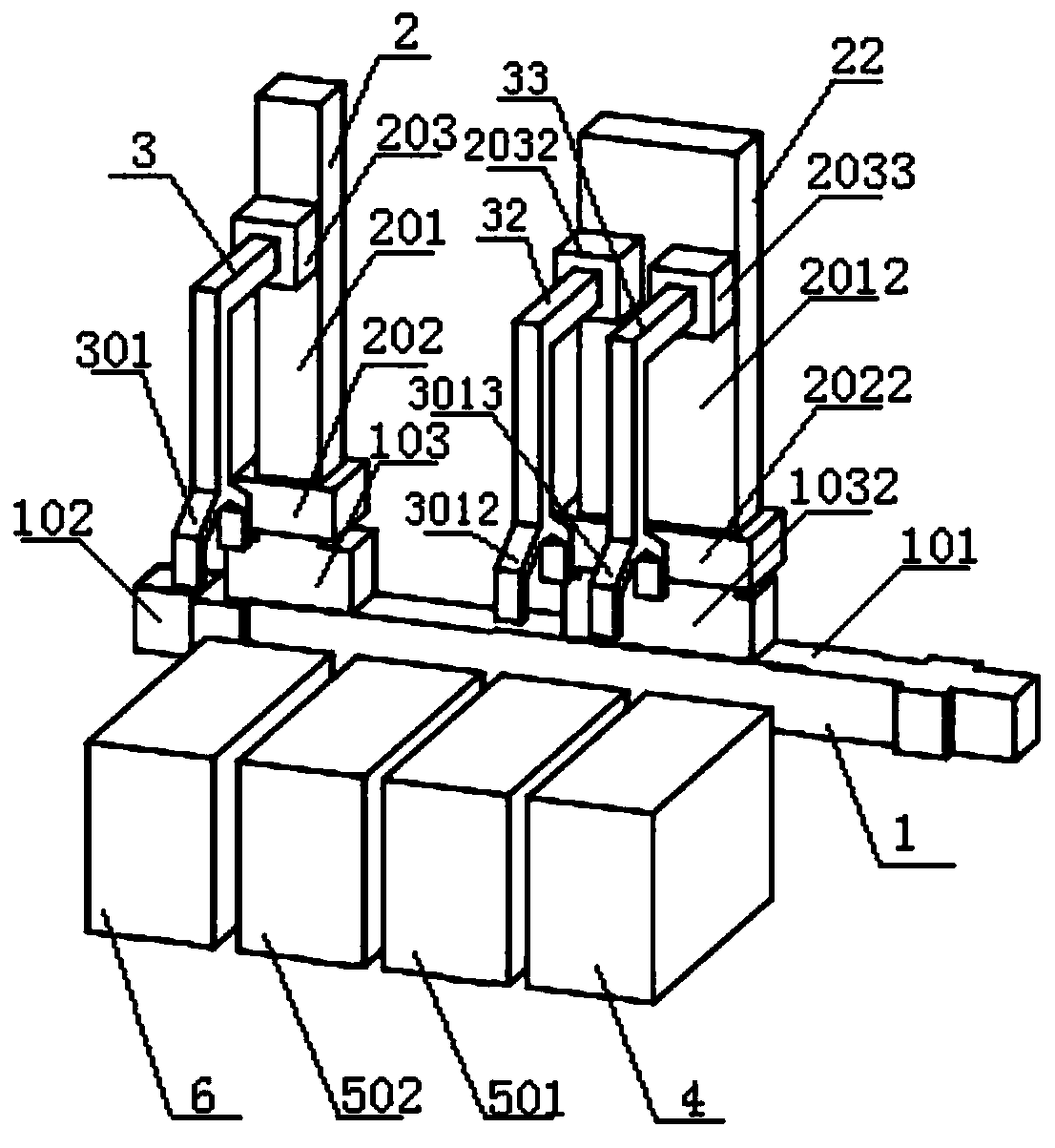
[0054] Such as image 3 Shown is the third embodiment of a CMP equipment cleaning module provided by the present invention. Compared with the first embodiment, the third embodiment includes a second Z-axis moving module 22 and a second A jaw gripping arm module 32 and a third jaw gripping arm module 33 . The wafer transfer device of the CMP equipment cleaning module provided in this embodiment includes an X-axis moving module 1, a Z-axis moving module 2, a second Z-axis moving module 22, a jaw clamping arm module 3 and a second jaw clamping arm Module 32 and the third claw clamping arm module 33; the X-axis moving module 1 is located on one side of the CMP equipment cleaning module, and the X-axis moving module includes an X transmission shaft 101, an X-axis driver 102, and an X-axis moving slider 103. The second X-axis moving slider 1032, the X-axis moving slider 103 and the second X-axis moving slider 1032 move independently on the X transmission axis 101; the Z-axis moving...


PUM


Abstract

The invention discloses a wafer transmission device, a wafer transmission method and a CMP equipment cleaning module, and the wafer transmission device comprises at least one clamping jaw clamping armmodule which is used for taking and placing a wafer; at least one Z-axis moving module, wherein the Z-axis moving modules are connected with the clamping jaw clamping arm modules and used for achieving movement of the clamping jaw clamping arm modules in the Z-axis direction; at least one X-axis moving module, wherein the X-axis moving modules are connected with the lower ends of the Z-axis moving modules and used for achieving movement of the clamping jaw clamping arm modules in the Z-axis direction. The X-axis moving modules are mounted at the lower ends of the Z-axis moving modules, the overall gravity center of the wafer conveying device is lowered, the possibility that impurity particles on the wafer conveying device fall onto a wafer is reduced, the cleaning effect of the wafer is improved, meanwhile, the number of the X-axis moving modules and the number of the Z-axis moving modules are increased, and the wafer conveying time is shortened.

Description

technical field [0001] The invention relates to the field of equipment for manufacturing semiconductor integrated circuit chips, in particular to a wafer transmission device, a transmission method and a CMP equipment cleaning module. Background technique [0002] Chemical Mechanical Planarization (CMP) equipment generally includes a semiconductor equipment front-end system (EFEM), a cleaning system and a polishing system. Wafers are transferred between systems by robotic handlers. Among them, there will be several units for cleaning the wafer in the cleaning system, and the wafer needs to be cleaned through each unit in turn. In this process, a device for moving the wafer is required to complete the task of moving the wafer. The claw clamping arm puts the wafers to be cleaned into the cleaning module, and takes out the cleaned wafers from the unit. The entire device needs to be kept highly clean. The existing devices use the transmission device to be installed in a suspende...

Claims


Application Information

Patent Timeline
Patent Type & Authority Applications(China)
IPC IPC(8): H01L21/677H01L21/67
CPCH01L21/67757H01L21/67754H01L21/67742H01L21/67092H01L21/67706H01L21/67028H01L21/68721H01L21/68707H01L21/67219H01L21/67766H01L21/6838H01L21/67H01L21/67748H01L21/67173H01L21/67057H01L21/67034
Inventor 杨渊思沈凌寒周智鹏
Owner HANGZHOU ZHONGGUI ELECTRONICS TECH CO LTD
Why Eureka
Try Eureka