Display panel and display device

A display panel and display area technology, which is applied in the direction of identification devices, instruments, semiconductor devices, etc., and can solve the problems of poor display uniformity of the display panel

Active Publication Date: 2020-08-11
BOE TECH GRP CO LTD
View PDF10 Cites 14 Cited by
  • Summary
  • Abstract
  • Description
  • Claims
  • Application Information

AI Technical Summary

Problems solved by technology

[0005] Embodiments of the present invention provide a display panel and a display device to solve the problem of poor display uniformity of the display panel in the prior art

Method used


Image

  • Display panel and display device
  • Display panel and display device
  • Display panel and display device

Examples


Embodiment Construction

[0029] In order to make the object, technical solution and advantages of the present invention more clear, the specific implementation manners of the display panel and the display device provided by the embodiments of the present invention will be described in detail below with reference to the accompanying drawings.

[0030] The film thickness and shape of each layer in the drawings do not reflect the real scale of the display panel, but are only intended to schematically illustrate the content of the present invention.

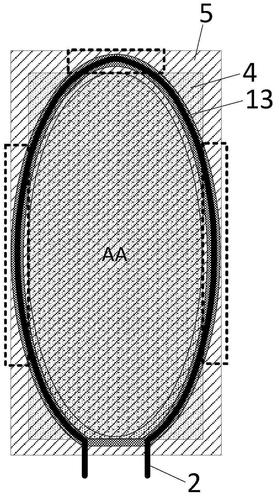
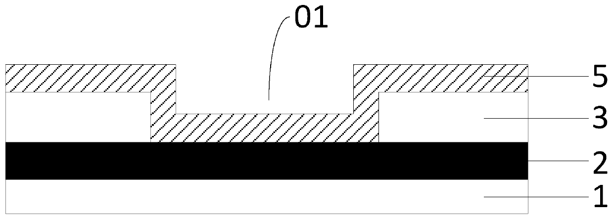
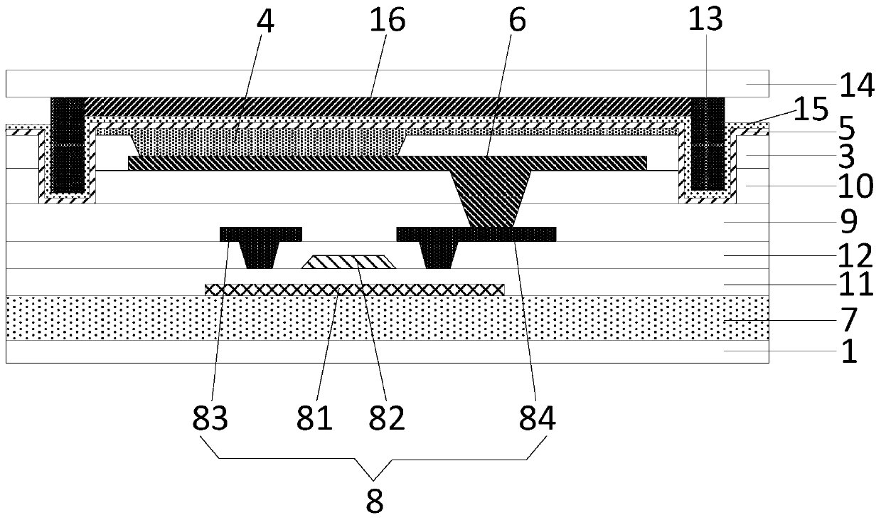
[0031] A display panel provided by an embodiment of the present invention, such as figure 1 with figure 2 As shown, there is a display area AA and a non-display area surrounding the display area AA (the area around the AA area), figure 1 It is a schematic diagram of the top view structure of some film layers in the display panel, figure 2 for figure 1 Schematic diagram of the cross-sectional structure of a part of the film layer in the area circled by t...


PUM


Abstract

The invention discloses a display panel and a display device. The display panel comprises a substrate, a cathode signal line, an insulating layer, an organic functional layer and a cathode layer, wherein the cathode signal line, the insulating layer, the organic functional layer and the cathode layer are sequentially stacked on the substrate; the cathode signal line is arranged around the displayarea, the organic functional layer is at least located in the display area, and the cathode layer is arranged on the whole surface; the cathode signal line and the organic functional layer have non-overlapping areas, the insulating layer has a hollow structure in the non-overlapping areas, and the cathode signal line is electrically connected with the cathode layer through the hollow structure. Acathode signal line which is arranged on a different layer from a cathode layer, is electrically connected with the cathode layer and surrounds a display area is arranged; the contact area of the cathode signal line and the cathode layer is increased; the equivalent resistance at the joint of the cathode signal line and the cathode layer is reduced, so that the drop amplitude of the cathode voltage at the position far away from the signal source is reduced, the cathode signal is input into the cathode layer through the cathode signal line, the resistance voltage drop on the cathode layer is reduced, and the display uniformity of the display panel is improved.

Description

technical field [0001] The invention relates to the field of flexible display technology, in particular to a display panel and a display device. Background technique [0002] In the field of display, organic light-emitting display panel (Organic Light-Emitting Diode, OLED) has gradually become the mainstay in the field of display due to its excellent performance such as low power consumption, high color saturation, wide viewing angle, thin thickness, and flexibility. Mainstream, it can be widely used in terminal products such as smartphones, tablets, and TVs. [0003] In the prior art, an OLED display panel includes an anode (Anode) layer, a cathode (Cathode) layer, and an organic functional layer located between the anode and the cathode. The organic functional layer is fabricated on the anode layer by evaporation or inkjet printing of a precision metal mask (FMM Fine Metal Mask, FMM), and then the cathode layer is fabricated by evaporation on the entire surface. [0004]...

Claims


Application Information

Patent Timeline
Patent Type & Authority Applications(China)
IPC IPC(8): H01L27/32G09F9/30
CPCG09F9/301H10K59/131H10K59/1315H10K59/122H10K59/124H10K59/80521H10K59/8723H10K59/871Y02E10/549
Inventor 徐攀林奕呈张星韩影
Owner BOE TECH GRP CO LTD
Why Eureka
Try Eureka