Display panel, preparation method thereof and spliced screen

A technology for display panels and display areas, applied in electrical components, electrical solid state devices, circuits, etc., and can solve problems such as poor transistor characteristics and uniformity

Active Publication Date: 2020-08-25
BOE TECH GRP CO LTD
View PDF8 Cites 8 Cited by
  • Summary
  • Abstract
  • Description
  • Claims
  • Application Information

AI Technical Summary

Problems solved by technology

[0003] Embodiments of the present invention provide a display panel and its preparation method and a splicing screen, which are used to solve the problem of poor transistor characteristics and uniformity caused by the interference of the fan-out leads on the active layer of the transistor in the related art

Method used


Image

  • Display panel, preparation method thereof and spliced screen
  • Display panel, preparation method thereof and spliced screen
  • Display panel, preparation method thereof and spliced screen

Examples


Embodiment Construction

[0038] The following will clearly and completely describe the technical solutions in the embodiments of the present invention with reference to the accompanying drawings in the embodiments of the present invention. Obviously, the described embodiments are only some, not all, embodiments of the present invention. Based on the embodiments of the present invention, all other embodiments obtained by persons of ordinary skill in the art without making creative efforts belong to the protection scope of the present invention.

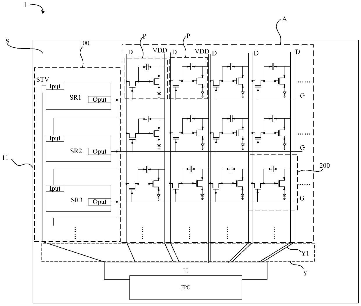
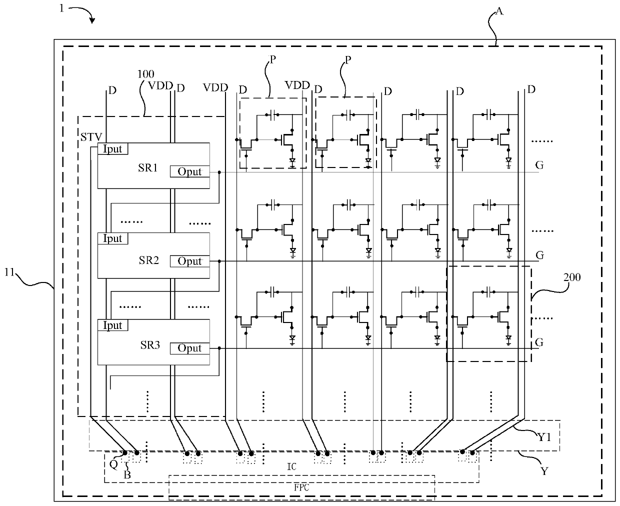
[0039] In the process of realizing large-size or super-large-size display screens through splicing and connection of multiple small screens in related technologies, take an independent small-screen display panel as an example, such as figure 1 As shown, the display panel 1 includes a display area A and a peripheral area S arranged around the display area A. The display area A is provided with a plurality of sub-pixels P. Arrangement, the sub-pixels P arranged ...


PUM


Abstract

The invention relates to the technical field of display, in particular to a display panel, a preparation method thereof and a spliced screen. The invention is to solve the problems of poor characteristics and uniformity of a transistor due to the fact that an active layer and a signal line of the transistor are interfered by a fan-out lead in the prior art. The provided display panel is provided with a display area. The display panel comprises a fan-out lead area, wherein the fan-out lead area is arranged in the display area; the fan-out lead which is arranged on the substrate and is positioned in the fan-out lead area; a pixel driving circuit which is arranged on one side, far away from the substrate, of the fan-out lead, and comprises a transistor; and an electric field shielding patternwhich is arranged between the pixel driving circuit and the fan-out lead, the orthographic projection of the electric field shielding pattern on the substrate at least covering an active layer of thetransistor in the fan-out lead area, and the electric field shielding pattern being used for accessing a constant voltage and shielding an interference signal acting on the active layer by the fan-out lead.

Description

technical field [0001] The invention relates to the field of display technology, in particular to a display panel, a preparation method thereof, and a splicing screen. Background technique [0002] Due to the limitations of the current technology level of self-luminous devices, it is still difficult to manufacture large-size and super-large-size display screens. Splicing and connecting multiple small screens is the main method to realize large-size and super-size display screens. Contents of the invention [0003] Embodiments of the present invention provide a display panel, a manufacturing method thereof, and a splicing screen, which are used to solve the problem in the related art that the transistor's active layer is disturbed by the fan-out lead and the characteristics and uniformity of the transistor are poor. [0004] In order to achieve the above object, embodiments of the present invention adopt the following technical solutions: [0005] In one aspect, an embodi...

Claims


Application Information

Patent Timeline
Patent Type & Authority Applications(China)
IPC IPC(8): H01L27/32
CPCH10K59/123H10K59/1213H10K59/1315H10K59/126H10K59/122H10K59/131H10K59/18H10K59/1201H01L25/167H01L25/0753H01L33/62
Inventor 史鲁斌滕万鹏陈亮秦斌王珂彭锦涛张方振彭宽军
Owner BOE TECH GRP CO LTD
Why Eureka
Try Eureka