

Display panel and display device
A display panel and optical path technology, which is applied in the direction of electric solid-state devices, semiconductor devices, diodes, etc., can solve the problems of device efficiency decline, etc., and achieve the effects of enhancing brightness, enhancing luminous brightness, and enhancing luminous effect
- Summary
- Abstract
- Description
- Claims
- Application Information
AI Technical Summary
Problems solved by technology
Method used
Image

Examples
Embodiment 1
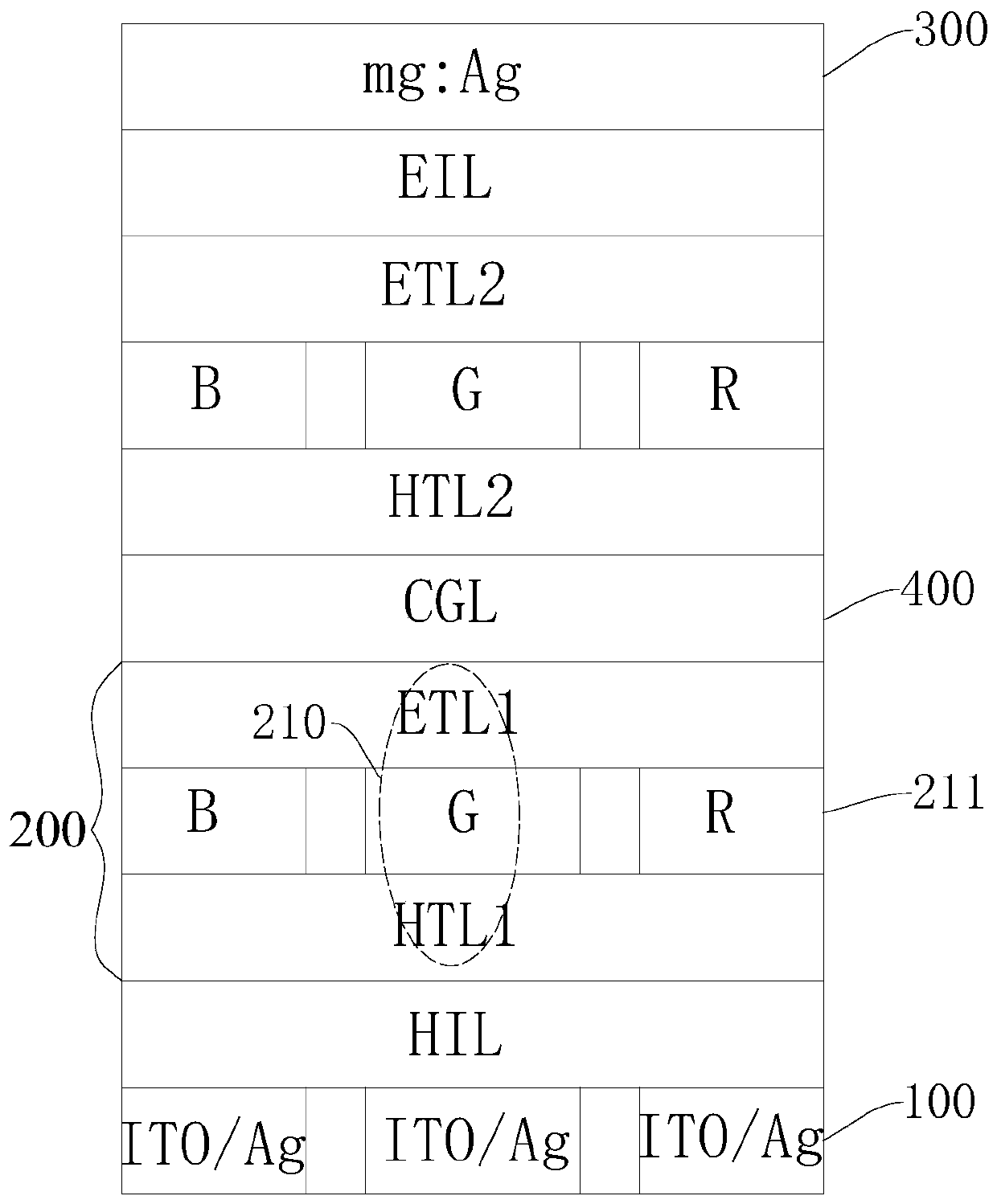
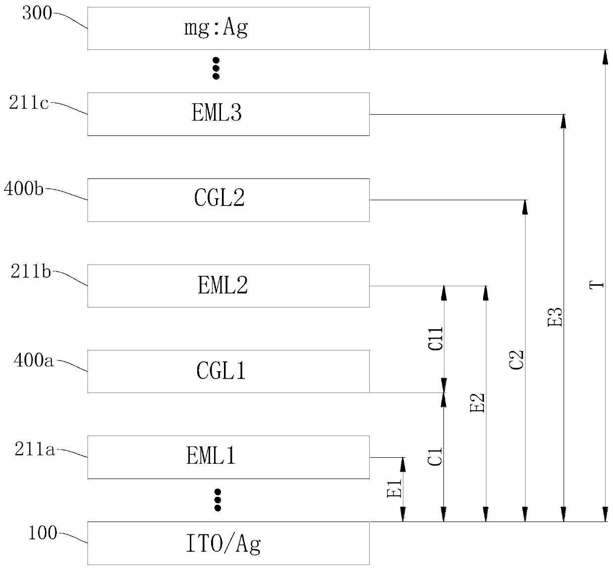
[0146] Please also refer to Image 6 , the display panel includes two light emitting structure layers 200 , the two light emitting structure layers 200 are stacked on each other, and a charge generation layer 400 is disposed between the two light emitting structure layers 200 . The two light-emitting structure layers 200 respectively include two light-emitting layers 211, and the two light-emitting layers 211 are respectively a first light-emitting layer 211a and a second light-emitting layer 211b.
[0147] In the display panel shown in Embodiment 1, the first optical path, the second optical path and the third optical path in the display panel are constructed according to the above formulas (1), (3) and (5).
[0148] m in the first optical path E1 between the first electrode layer 100 and the first light-emitting layer 211a 1 The value is 2, that is, the first optical path E1 between the first electrode layer 100 and the first light-emitting layer 211a is λ / 2, and the first ...
Embodiment 2
[0158] Based on the layer structure of the display panel in Embodiment 1, the position of the second light emitting layer 211b is gradually changed, so that the first optical path between the second light emitting layer 211b and the first electrode layer 100 gradually deviates. The display panel in Example 1 is made to emit red light, and the measured parameters are shown in the table below:
[0159]
[0160] Where THK is the distance between the second light emitting layer 211b and the first electrode layer 100 when the optical distance between the second light emitting layer 211b and the first electrode layer 100 is λ.
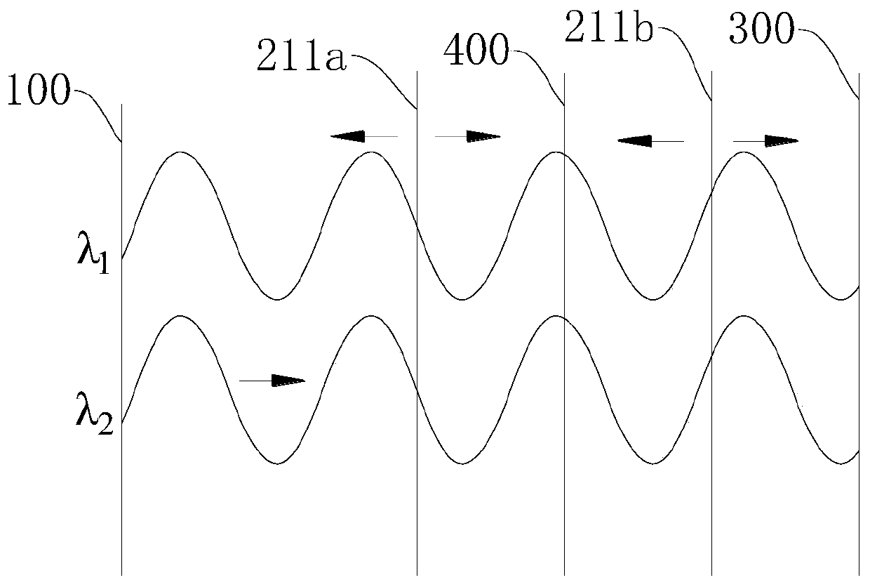
[0161] Please also refer to Figure 10 , set the position of the second light-emitting layer 211b according to the above table, and obtain the spectrum of the green light emitted by the second electrode layer 300, and obtain the spectrum of the green light as Figure 10 as shown, Figure 10 The abscissa of is the emission wavelength, and the ordinate is t...
Embodiment 3
[0163] The display panel in Example 1 is made to emit red light, and the display panel is at the target brightness, and the parameters in Example 1 are obtained as shown in the table below.
[0164]
[0165] Please also refer to Figure 11 , the spectrum of the red light emitted by the second electrode layer 300 of the display panel is measured, and the spectrum of the red light is obtained as Figure 11 as shown, Figure 11 The abscissa of is the emission wavelength, and the ordinate is the normalized luminescence intensity. Depend on Figure 11 It can be seen from the above table that the red light is a single peak, and the current efficiency is 82.95cd / A.
[0166] It can be seen from the above embodiments and test results that the embodiments of the present invention can not only enhance the luminous brightness of the same color, but also enhance the luminous effect.
[0167] An embodiment of the present invention further provides a display device, and the display de...
PUM
| Property | Measurement | Unit |
|---|---|---|
| current efficiency | aaaaa | aaaaa |
| current efficiency | aaaaa | aaaaa |
Abstract
Description
Claims
Application Information