
A kind of glue coating method of ultra-thin wafer with taiko ring structure as substrate

An ultra-thin, wafer-based technology, applied in coatings, devices for coating liquid on the surface, electrical components, etc., can solve problems such as difficult removal, liquid backsplash, photoresist accumulation, etc., to avoid photoresist The effect of accumulation, avoiding liquid splashing and improving uniformity

Active Publication Date: 2022-07-08
SHENYANG KINGSEMI CO LTD
View PDF10 Cites 0 Cited by
  • Summary
  • Abstract
  • Description
  • Claims
  • Application Information

AI Technical Summary

Problems solved by technology

[0005] However, the above-mentioned method and the glue-spinning step in the existing wafer gluing process formula are generally traditional low-speed-high-speed simple structures, and this formula is very easy to make the wafer surface photoresist when coating a taiko ring with a special substrate. Coating is uneven, film thickness stability is difficult to control, and the junction of taiko ring and plane is easy to cause photoresist accumulation and liquid backsplash, which is difficult to remove later

Method used


Image

  • A kind of glue coating method of ultra-thin wafer with taiko ring structure as substrate
  • A kind of glue coating method of ultra-thin wafer with taiko ring structure as substrate

Examples


Embodiment 1

[0055] Coating photoresist on a wafer with a thinned part of 50 μm and a diameter of 200 nm, the viscosity of the photoresist is 34cp (centipoise), including the following steps:

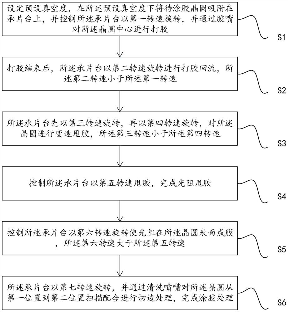
[0056] S1a: vacuum suction the wafer onto the wafer stage, control the preset vacuum degree of the wafer stage to 40KPa, and the exhaust air volume in the gluing chamber to be 30m / s. The wafer stage operates at a first high speed of 1000r / s. Rotate for 10s, while the glue nozzle glues the center of the wafer;

[0057] S2a: After the gluing is completed, the wafer stage is rotated at a first low speed of 100r / s for 5s to reflow the gluing;

[0058] S3a: the film carrier rotates at the second low speed of 100r / s for 10s, and then rotates at the second high speed of 1500r / s for 5s to perform variable-speed glue rejection;

[0059] S4a: the wafer stage is rotated at the third low speed of 100r / s for 5s to complete the photoresist ejection;

[0060] S5a: the wafer stage is rotated at a third high speed...

Embodiment 2

[0064] Coating photoresist on a wafer with a thinned part of 80 μm and a diameter of 200 nm, the viscosity of the photoresist is 34cp (centipoise), including the following steps:

[0065] S1b: The wafer is vacuum-adsorbed on the wafer stage, the preset vacuum degree of the wafer stage is controlled to 20KPa, the exhaust air volume in the gluing chamber is 40m / s, and the wafer stage is controlled at the first high speed of 800r / s. Rotate for 10s, while the glue nozzle glues the center of the wafer;

[0066] S2b: After the gluing is completed, the wafer stage is rotated at the first low speed of 100r / s for 5s to reflow the gluing;

[0067] S3b: the film carrier rotates at the second low speed of 100r / s for 10s, and then rotates at the second high speed of 1600r / s for 5s to perform variable-speed glue rejection;

[0068] S4b: The wafer stage is rotated at a third low speed of 100r / s for 5s to complete the photoresist spin;

[0069] S5b: the wafer stage is rotated at a third hig...

Embodiment 3

[0073] Apply photoresist to a wafer with a thickness of 100 μm and a diameter of 200 nm at the thinned part. The viscosity of the photoresist is 34 cP (centipoise), including the following steps:

[0074] S1c: The wafer is vacuum-adsorbed on the wafer stage, the preset vacuum degree of the wafer stage is controlled to be 10KPa, the exhaust air volume in the gluing chamber is 40m / s, and the wafer stage is controlled at the first high speed of 700r / s. Rotate for 10s, while the glue nozzle glues the center of the wafer;

[0075] S2c: After the gluing is completed, the wafer stage is rotated at the first low speed of 100r / s for 5s to reflow the gluing;

[0076] S3c: the film carrier rotates at the second low speed of 100r / s for 10s, and then rotates at the second high speed of 1700r / s for 5s to perform variable-speed gluing;

[0077] S4c: the wafer stage is rotated at a third low speed of 100r / s for 5s to complete the photoresist spin;

[0078] S5c: the wafer stage rotates at a ...


PUM


Abstract

The invention provides a method for gluing an ultra-thin wafer with a taiko ring structure as a substrate, which comprises the following steps: setting a preset vacuum degree, and adsorbing the wafer to be coated on the support under the preset vacuum degree On the wafer stage, the wafer stage is controlled to rotate at the first speed, and the center of the wafer is glued through the glue nozzle; after the gluing is completed, the wafer stage rotates at the second speed for glue reflow, and the second speed is lower than the first speed. 1 rotation speed; the wafer stage first rotates at the third rotation speed, and then rotates at the fourth rotation speed, and the third rotation speed is less than the fourth rotation speed, and the wafer is subjected to variable-speed glue rejection; the wafer stage is controlled to be ejected at the fifth rotation speed to complete the lithography Then control the wafer carrier to rotate at the sixth rotational speed to form a film of photoresist on the wafer surface, and the fifth rotational speed is less than the sixth rotational speed; the wafer carrier rotates at the seventh rotational speed, and cleans the wafer from the wafer through the cleaning nozzle. Scanning from the first position to the second position to perform edge trimming processing can improve the uniformity of the photoresist on the wafer surface and avoid photoresist accumulation and liquid backsplash.

Description

technical field [0001] The invention relates to the technical field of semiconductor lithography, in particular to a method for gluing an ultra-thin wafer with a taiko ring structure as a substrate. Background technique [0002] As the development of electronic products tends to be multi-functional integration and miniaturization, the requirements for portability are getting higher and higher. This requires circuit chips to continue to develop in the direction of high density, high performance, light, thin and short, which requires the continuous reduction of the thickness of the chip package. Taking memory as an example, its packaging form is mainly stacked packaging. With the continuous increase of storage capacity , the number of layers of the package has reached more than 96 layers. In order to meet the requirements of advanced IC packaging, the thickness of each layer of chips in the stack inevitably needs to be reduced when the overall thickness of the package remains ...

Claims


Application Information

Patent Timeline
Patent Type & Authority Patents(China)
IPC IPC(8): B05D1/26B05C11/08B05C13/02B05B15/50H01L21/67
CPCB05D1/26B05C11/08B05C13/02B05B15/50H01L21/6715
Inventor 李庆斌朴勇男邢栗张晨阳
Owner SHENYANG KINGSEMI CO LTD
Learn More