

Display panel and display device
A display panel and display function technology, applied in the direction of instruments, electrical digital data processing, electrical components, etc., can solve the problems of touch signal noise and low touch sensitivity of the touch layer, so as to improve sensitivity and enhance user experience , the effect of reducing noise and influence
- Summary
- Abstract
- Description
- Claims
- Application Information
AI Technical Summary
Problems solved by technology
Method used
Image

Examples
Embodiment 1
[0040] An embodiment of the present invention provides a display device, the display device has a display panel 1, and the display panel 1 provides a display screen for the display device. The display device may be any display device with a display function, such as a mobile phone, a notebook computer, a television, and the like.
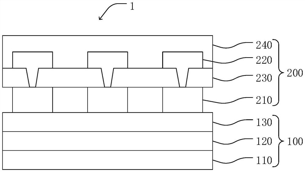
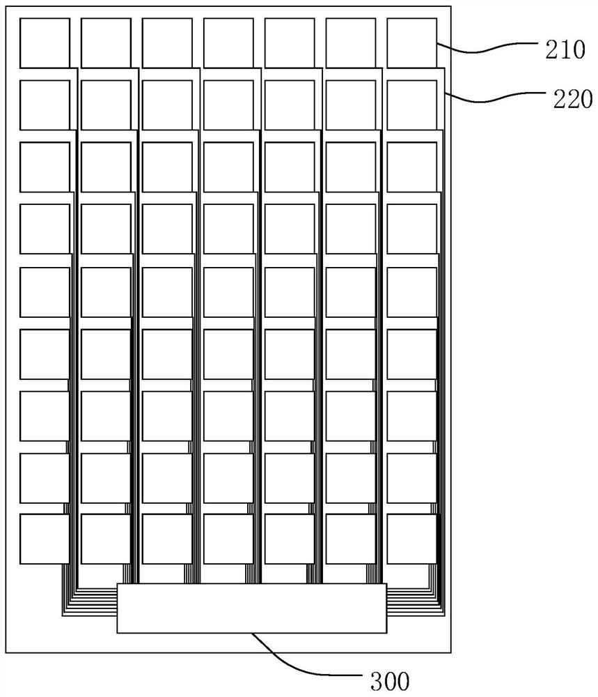
[0041] Such as figure 1 As shown, the display panel 1 includes an organic light emitting structure layer 100 , a touch layer 200 and a driving chip 300 . The touch control layer 200 is disposed on a surface of the organic light emitting structure layer 100 , and the driving chip 300 is electrically connected to the touch control layer 200 .
[0042] The organic light emitting structure layer 100 includes a light emitting layer 110 , a cathode 120 and an encapsulation layer 130 . There are several organic electroluminescent devices in the light emitting layer 110, and the organic electroluminescent devices provide light sources for the display pane...
Embodiment 2
[0051] An embodiment of the present invention provides a display device, the display device has a display panel 1, and the display panel 1 provides a display screen for the display device. The display device may be any display device with a display function, such as a mobile phone, a notebook computer, a television, and the like.
[0052] Such as figure 1 As shown, the display panel 1 includes an organic light emitting structure layer 100 , a touch layer 200 and a driving chip 300 . The touch control layer 200 is disposed on a surface of the organic light emitting structure layer 100 , and the driving chip 300 is electrically connected to the touch control layer 200 .
[0053] The organic light emitting structure layer 100 includes a light emitting layer 110 , a cathode 120 and an encapsulation layer 130 . There are several organic electroluminescent devices in the light emitting layer 110, and the organic electroluminescent devices provide light sources for the display pane...
Embodiment 3
[0062] An embodiment of the present invention provides a display device, the display device has a display panel 1, and the display panel 1 provides a display screen for the display device. The display device may be any display device with a display function, such as a mobile phone, a notebook computer, a television, and the like.
[0063] Such as figure 1 As shown, the display panel 1 includes an organic light emitting structure layer 100 , a touch layer 200 and a driving chip 300 . The touch control layer 200 is disposed on a surface of the organic light emitting structure layer 100 , and the driving chip 300 is electrically connected to the touch control layer 200 .
[0064]The organic light emitting structure layer 100 includes a light emitting layer 110 , a cathode 120 and an encapsulation layer 130 . There are several organic electroluminescent devices in the light emitting layer 110, and the organic electroluminescent devices provide light sources for the display panel...
PUM
| Property | Measurement | Unit |
|---|---|---|
| width | aaaaa | aaaaa |
Abstract
Description
Claims
Application Information