Transistor and forming method thereof

A technology of transistors and dielectric layers, applied in semiconductor devices, semiconductor/solid-state device manufacturing, electrical components, etc., can solve the problems of transistor reliability influence, transistor instability, transistor static power consumption increase, etc., to improve gate induction Leakage current, the effect of overcoming gate-induced leakage current

Pending Publication Date: 2020-09-08
FUJIAN JINHUA INTEGRATED CIRCUIT CO LTD
View PDF0 Cites 1 Cited by
  • Summary
  • Abstract
  • Description
  • Claims
  • Application Information

AI Technical Summary

Problems solved by technology

[0003] Specifically, as the transistor device becomes thinner and thinner, the gate-induced drain leakage (GIDL) generated by the transistor in the off state or in the waiting state becomes more and more

Method used


Image

  • Transistor and forming method thereof
  • Transistor and forming method thereof
  • Transistor and forming method thereof

Examples


Embodiment 1

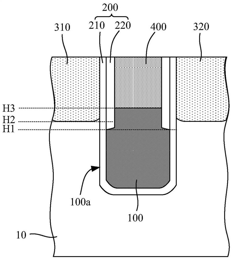
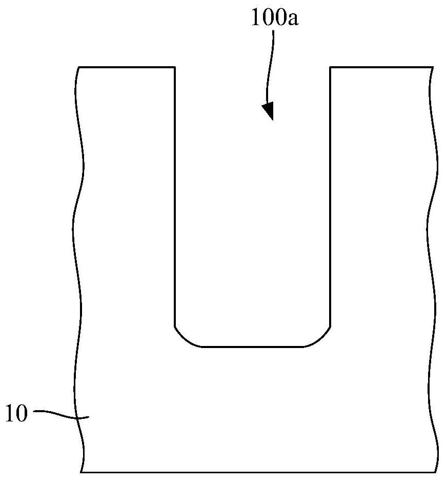
[0070] Figure 1a is a schematic structural diagram of a transistor in Embodiment 1 of the present invention, Figure 1b It is a schematic structural diagram of the gate dielectric layer of the transistor in Embodiment 1 of the present invention. like Figure 1a and Figure 1b As shown, the transistor includes: a substrate 10 in which a gate trench 100a is formed; and a gate dielectric layer 200 covering the inner wall of the gate trench 100a.

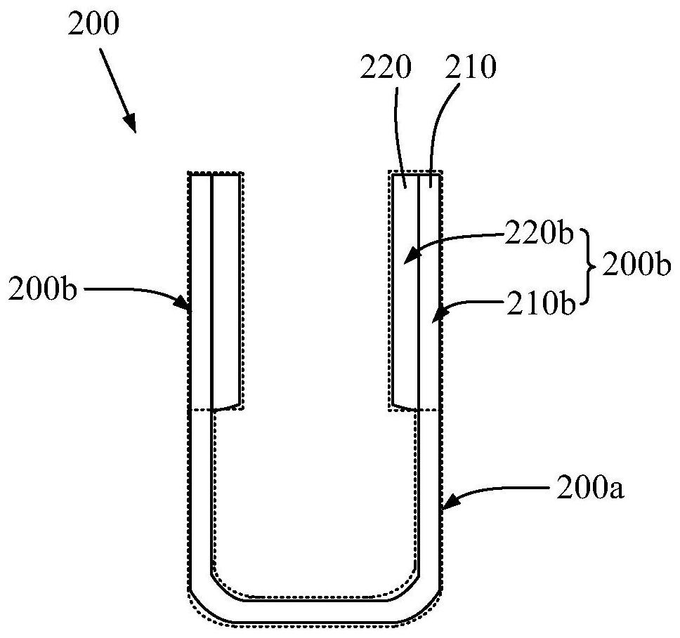
[0071] key reference Figure 1b and combine Figure 1a As shown, the gate dielectric layer 200 has an upper layer part 200b and a lower layer part 200a, and the upper layer part 200b covers the inner wall of the gate trench 100a higher than the predetermined height position (ie, the first height position H1), so The lower portion 200 a covers the inner wall of the gate trench 100 a lower than the predetermined height position (ie, the first height position H1 ).

[0072] Wherein, the upper layer part 200b is a laminated structure, s...

Embodiment 2

[0113] The difference from Embodiment 1 is that, in the gate dielectric layer in this embodiment, the upper portion protrudes toward the inner wall of the trench relative to the lower portion. Combine the following Figure 3a and Figure 3b The transistors in this embodiment will be described in detail.

[0114] Figure 3a It is a schematic structural diagram of the transistor in Embodiment 2 of the present invention, Figure 3b It is a schematic structural diagram of the gate dielectric layer of the transistor in the second embodiment of the present invention. like Figure 3a and Figure 3b As shown, in this embodiment, the gate dielectric layer 200' includes a first dielectric layer 210' and a second dielectric layer 220'.

[0115] Wherein, the first dielectric layer 210' covers the inner wall of the gate trench 100a' higher than the predetermined height position (the first height position H1), and is used to form the lining layer 210b' of the upper part 200b'. The se...


PUM


Abstract

The invention provides a transistor, a forming method thereof and a semiconductor device. The gate dielectric layer in the transistor is provided with an upper layer part and a lower layer part, and the upper layer part is laminated, so that the thickness of the upper layer part can be increased on the basis of not changing the thickness of the lower layer part. Therefore, on the basis of maintaining the performance of the transistor, the gate induced leakage current (GIDL) phenomenon can be improved; and moreover, the thickness of the upper layer part is increased through laminated arrangement, so that flexible adjustment of parameters of the upper layer part is facilitated.

Description

technical field [0001] The invention relates to the technical field of semiconductors, in particular to a transistor and a forming method thereof. Background technique [0002] With the continuous shrinking of the size of semiconductor devices, the feature size of field effect transistors is also shrinking rapidly, and the thickness of the corresponding gate dielectric layer is also getting thinner. The problem of device reliability and performance caused by the thin gate dielectric layer is also increasingly prominent. [0003] Specifically, as the transistor device becomes thinner and thinner, the gate-induced drain leakage (GIDL) generated by the transistor in the off state or in the waiting state becomes more and more serious, which will affect the reliability of the transistor. Sexuality has a greater impact, resulting in the instability of the transistor and the increase in the static power consumption of the transistor. Therefore, as the feature size of transistors ...

Claims


Application Information

Patent Timeline
IPC IPC(8): H01L29/423H01L21/28
CPCH01L21/28229H01L29/4236H01L29/42368
Inventor 周仲彦陈志远
Owner FUJIAN JINHUA INTEGRATED CIRCUIT CO LTD
Why Eureka
Try Eureka