Light-emitting diode and packaging method of light-emitting diode

A technology of light emitting diodes and mounting grooves, applied in electrical components, circuits, semiconductor devices, etc., can solve the problems of large packaging volume, unstable packaging, and complicated process, and achieves optimization of production process, improvement of production efficiency, and increase of contact bonding. area effect

Inactive Publication Date: 2020-09-11
赵光宇
View PDF0 Cites 0 Cited by
  • Summary
  • Abstract
  • Description
  • Claims
  • Application Information

AI Technical Summary

Problems solved by technology

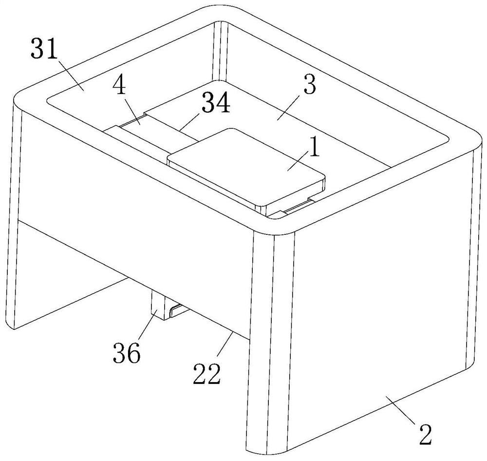
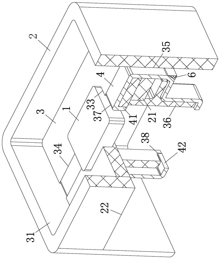
[0007] The technical solution adopted by the present invention to solve its technical problems is: a light-emitting diode according to the present invention includes a light-emitting diode chip; the outside of the light-emitting diode chip is provided with a lead cavity matched with it, and the upper and lower sides of the lead cavity The two ends are connected, and the two inner walls corresponding to the lead cavity along the length direction are symmetrically provided with support plates, and the inside of the lead cavity is installed with a supporting plate capable of sealing the opening of the cavity, and the supporting plate and A glue filling groove is formed between the side walls of the lead cavity, and the inside of the glue filling groove is filled with colloid; the middle part of the top surface of the supporting plate is provided with a mounting groove matching with the light-emitting diode chip, and the top surface of the supporting plate is symmetrical There is a connection groove connected with the end of the supporting plate and the side wall of the installation groove. A long strip-shaped conductive strip that can be bent freely is bonded inside the connection groove. The inner end of the conductive strip is connected to the side wall of the installation groove. The connecting groove and the outer end of the support plate are respectively provided with through-type slots, the outer end of the conductive strip passes through the slot and is located under the supporting plate, and the bottom surface of the supporting plate is symmetrically provided with T-shaped plate, the outer end side wall of the conductive strip is attached to the T-shaped plate side wall, and the outer end of the conductive strip, the bottom end of the vertical side wall at the T-shaped plate and the bottom of the lead cavity The end faces are flush with each other; the bottom of the lead cavity is provided with a connecting plate that matches it, and a welding port that can weld the conductive strip and the connecting plate is opened on the side wall of the lead cavity; when working, the light-emitting diode There are problems of large package volume, cumbersome process and unstable package when the pin-insert package is used, while the finished product of the surface mount package is small in size, but the production cost is high and the production is difficult; and the above two All packaging methods need to pre-connect the light-emitting diode chip and the metal wire, which not only reduces the production efficiency of the light-emitting diode, but also easily causes problems such as poor contact caused by the weak connection between the two; and the light-emitting diode in the present invention is in production , first attach the conductive strips to the inside of the connection grooves on the supporting plate and make the inner ends of the conductive strips flush with the side walls of the installation grooves, then insert the supporting plates into the lead cavity and support them on both sides Cooperate under the action of the board and form a glue filling groove. At this time, the outer ends of the conductive strips are respectively passed through the through-type slots set on the supporting plate and the support plate, and then the conductive strips passing through the slots are pressed on the The T-shaped plate and the side walls of the two are attached together. At this time, the conductive strips and the supporting plate are pre-fixed in the lead cavity by the conductive strips that are attached to the horizontal side walls on the T-shaped plate and are bent. The loosening and detachment of the conductive strip and the supporting plate during the relative movement with the lead cavity in the subsequent packaging process effectively increases the stability of the conductive strip, the supporting plate and the lead cavity during assembly, and at the same time presses the conductive strip Behind the side wall of the T-shaped plate, the bottom end of the conductive strip is flush with the bottom end face of the lead cavity, so that the conductive strip and the corresponding electrode end on the connecting plate are welded and connected through the welding port; After the assembly is completed, insert the light-emitting diode chip into the installation groove on the support plate and connect the electrodes at both ends to the inner ends of the conductive strips, so that the two poles of the light-emitting diode chip can be easily and quickly connected by contacting the end of the conductive strip. It is connected to the outside, and at the same time, the two ends of the light-emitting diode chip located in the installation groove can be stably connected to the conductive strip, and then the glue is injected into the glue filling groove to complete the packaging of the light-emitting diode, and no other injection molding is required. Or the step of mold forming, which effectively improves the production efficiency and production quality of light-emitting diodes

Method used


Image

  • Light-emitting diode and packaging method of light-emitting diode
  • Light-emitting diode and packaging method of light-emitting diode
  • Light-emitting diode and packaging method of light-emitting diode

Examples


Embodiment approach

[0030] As an embodiment of the present invention, a bending groove 37 is provided at the junction of the connection groove 34 and the installation groove 33, and the inner end of the conductive strip 4 is provided with a bending groove that matches the bending groove 37. Folding portion 41; during work, in order to improve the contact and connection effect between the electrode terminals at both ends of the light-emitting diode chip 1 and the end of the conductive strip 4, at this time, a bending groove 37 is provided at the position where the connecting groove 34 and the installation groove 33 are handed over, At the same time, by inserting the pre-bent bending part 41 at the inner end of the conductive strip 4 into the inside of the bending groove 37, the contact bonding area between the end of the conductive strip 4 and the electrodes at both ends of the light-emitting diode chip 1 is effectively increased, and the light-emitting diode chip 1 is reduced. The electrodes at bo...


PUM


Abstract

The invention belongs to the technical field of diode packaging, and particularly relates to a light-emitting diode and a packaging method of the light-emitting diode. The light-emitting diode comprises a light-emitting diode chip, a lead cavity is arranged outside the light-emitting diode chip, and a supporting plate is installed inside the lead cavity and can form a glue pouring groove with thelead cavity. A mounting groove is formed in the middle of the top surface of the supporting plate, connecting grooves are symmetrically formed in the top surface of the supporting plate, conductive strips are bonded in the connecting grooves, slots are formed in the connecting grooves and the end surface of the outer end of the supporting plate, and a T-shaped plate is arranged on the bottom surface of the supporting plate; according to the invention, the supporting plate, the conductive strip and the lead wire cavity which can be matched with one another are arranged, so that the supporting plate and the lead wire cavity form a glue pouring groove for packaging after being assembled, and the production process of the light-emitting diode is greatly optimized; and meanwhile, the conductivestrips and the light-emitting diode chips are connected in a contact manner, so that the production efficiency of the light-emitting diode is effectively improved.

Description

technical field [0001] The invention belongs to the technical field of diode packaging, in particular to a light emitting diode and a packaging method of the light emitting diode. Background technique [0002] LED packaging uses brackets to carry chips, uses silver glue or metal connecting wires for internal and external electrical connections, and uses colloid for external protection and optical lens applications; packaging can protect light-emitting diodes and increase photoelectric performance, which is necessary for light-emitting diodes. [0003] Currently, most light-emitting diode semiconductor devices are packaged in pin-through and surface-mount packages. The pin insertion packaging process is as follows: use die-bonding glue to fix the chip on the metal bracket, and use metal wires to connect the electrodes. After realizing the electrical function connection, insert into the molding cavity and inject liquid epoxy resin; after the epoxy resin is cured , and release...

Claims


Application Information

Patent Timeline
Patent Type & Authority Applications(China)
IPC IPC(8): H01L33/48H01L33/52H01L33/62
CPCH01L33/48H01L33/52H01L33/62H01L2933/0033H01L2933/005H01L2933/0066
Inventor 赵光宇罗志康
Owner 赵光宇
Why Eureka
Try Eureka