Manufacturing method of semiconductor structure

A manufacturing method and semiconductor technology, applied in the fields of semiconductor/solid-state device manufacturing, semiconductor devices, electric solid-state devices, etc., can solve the problem that the performance of 3D packaging structure needs to be improved, and achieve the effect of preventing wrong cutting and improving performance.

Active Publication Date: 2020-09-22
CHANGXIN MEMORY TECH INC
View PDF6 Cites 1 Cited by
  • Summary
  • Abstract
  • Description
  • Claims
  • Application Information

AI Technical Summary

Problems solved by technology

[0004] However, the performance of the 3D packaging structure

Method used


Image

  • Manufacturing method of semiconductor structure
  • Manufacturing method of semiconductor structure
  • Manufacturing method of semiconductor structure

Examples


Example Embodiment

[0015] It can be known from the background art that the performance of the existing 3D semiconductor structure needs to be improved.
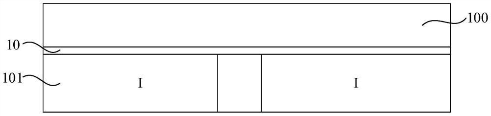
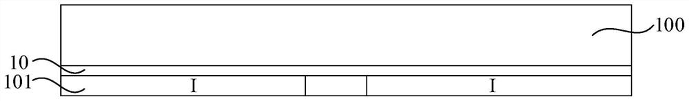
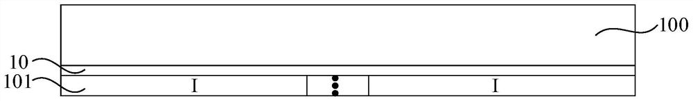
[0016] According to the analysis, the existing method of stack die is usually as follows: firstly, a single wafer is cut to form chips, and then the cut chips are stacked on another wafer. This method is called chip on wafer. The process steps of the chip on wafer method are complicated, and the corresponding cost is also higher. For this reason, it is hoped to propose a new cutting scheme, which is to stack multiple wafers and then perform a single cut.

[0017] However, further analysis found that as the number of stacked wafers in the 3D semiconductor structure increases, the thickness of the stacked semiconductor structure becomes thicker and thicker. It is difficult to effectively cut the semiconductor structure with a single cutting process, and it is easy to cause mis-cutting of chips, especially When there is a large alignment error bet...


PUM

PropertyMeasurementUnit
Thicknessaaaaaaaaaa

Abstract

The embodiment of the invention relates to a manufacturing method for a semiconductor structure, and the method comprises the steps: forming a wafer stacking structure which comprises at least two wafers, wherein each wafer comprises a plurality of chips; performing a cutting step on the wafer stacking structure, and after the cutting step of the wafer stacking structure, enabling the plurality ofchips in the wafer stacking structure to be in an unseparated state; and carrying out the chip separation step, so that the chips in the wafer stacking structure are separated. According to the invention, the mistaken cutting of the chip in the wafer can be effectively avoided, and the performance of the semiconductor structure is improved.

Description

technical field [0001] Embodiments of the present invention relate to the technical field of semiconductors, and in particular, to a method for manufacturing a semiconductor structure. Background technique [0002] In recent years, as semiconductor devices continue to respond to the demand for "faster, cheaper, and smaller", three-dimensional stacked 3D packaging technology has entered mainstream semiconductor manufacturing. Among them, TSV (Through Silicon Via) technology is interconnected through vertical chip vias, which brings shorter interconnection length and smaller packaging area, greatly improves signal transmission speed and reduces parasitic power consumption. [0003] The existing method for forming a three-dimensional stacked 3D packaging structure generally includes: stacking and bonding multiple wafers in a direction perpendicular to the surface of the wafer; and then cutting the bonded multiple wafers along the wafer dicing lane , to obtain several discrete ...

Claims


Application Information

Patent Timeline
IPC IPC(8): H01L25/065H01L21/78H01L21/98
CPCH01L25/0657H01L21/78H01L25/50
Inventor 吴秉桓全昌镐
Owner CHANGXIN MEMORY TECH INC
Why Eureka
Try Eureka