
Flash memory device, flash memory controller and flash memory storage management method

The technology of a flash memory controller and management method is applied in the field of flash memory devices and can solve the problems of low data storage rate and the like

Active Publication Date: 2020-09-25
SILICON MOTION TECH CORP
View PDF4 Cites 2 Cited by
  • Summary
  • Abstract
  • Description
  • Claims
  • Application Information

AI Technical Summary

Problems solved by technology

[0003] Generally speaking, for the flash memory controller to perform data writing to write a piece of data to a single-level unit data block or a multi-level unit data block, the traditional mechanism adopts, for example, at the end of a word line of a data block The check codes corresponding to the other data pages of the word line are placed on one page, so that the corresponding check codes can be used to perform a certain degree of error correction when writing failures, word line breaks, and word line short circuits occur. However, such data storage rate is too low, if for example a word line comprises 8 data pages, then only 7 data pages are used for storing data, and another data page is used for storing check code, like this, a 1 / 8 of the data block will be used to store the check code instead of storing data, which is unacceptable from the user's point of view

Method used


Image

  • Flash memory device, flash memory controller and flash memory storage management method
  • Flash memory device, flash memory controller and flash memory storage management method
  • Flash memory device, flash memory controller and flash memory storage management method

Examples


Embodiment Construction

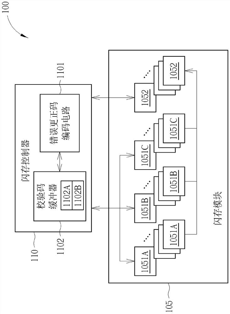
[0025] Please refer to figure 1 , figure 1 It is a schematic diagram of a flash memory device 100 according to an embodiment of the present invention. The flash memory device 100 includes a flash memory module 105 and a flash memory controller 110. The flash memory module 105 is a flash memory module with a two-dimensional planar structure; however, this is not a limitation of the present application. The flash memory module 105 includes a plurality of flash memory chips (not shown in figure 1 ), each flash memory chip includes a plurality of single-level cell data blocks (single-level cell (SLC) block, referred to as SLC data block) and a plurality of multi-layer unit data blocks (multiple-level-cell block), Each unit of a single-level unit data block can store 2 bits of data, and each unit of a multi-layer unit data block can store 2 N bit data, N is greater than or equal to 2 and is an integer, and the multi-level cell data block, for example, includes a two-layer cell d...


PUM


Abstract

The invention discloses a flash memory device and a flash memory storage management method. The flash memory storage management method comprises the following steps: providing a flash memory module, wherein the flash memory module comprises a plurality of single-layer unit data blocks and multi-layer unit data blocks; classifying the data to be written into a plurality of data groups; respectivelyexecuting single-layer unit data writing and executing similar fault-tolerant disk array error correction coding operation to generate corresponding check codes so as to write the plurality of data groups and the corresponding check codes into the plurality of single-layer unit data blocks; and when writing of the plurality of single-layer unit data blocks is completed, executing internal copying, and sequentially writing the plurality of data groups stored in the plurality of single-layer unit data blocks and the corresponding check codes into the multi-layer unit data blocks according to the storage sequence of the plurality of single-layer unit data blocks. Only an extremely low data space needs to be used for storing a corresponding error correction check code, so that the use efficiency of the flash memory data space is higher.

Description

[0001] The filing date of the original application is 2017.04.26, the application number is 201710283438.9, and the name of the invention is "flash memory device and flash memory storage management method". technical field [0002] The invention relates to a flash memory device, in particular to a flash memory device and a storage management method for performing error correction coding operations similar to fault-tolerant disk arrays. Background technique [0003] Generally speaking, for the flash memory controller to perform data writing to write a piece of data to a single-level unit data block or a multi-level unit data block, the traditional mechanism adopts, for example, at the end of a word line of a data block The check codes corresponding to the other data pages of the word line are placed on one page, so that when writing failure, word line break and word line short circuit occur, the corresponding check code can be used to perform a certain degree of error correcti...

Claims


Application Information

Patent Timeline
IPC IPC(8): G11C29/42G11C29/44G11C11/56G11C16/10G06F3/06G06F11/10G06F12/02G06F12/0804G11C16/26
CPCG06F3/0608G06F3/061G06F3/0629G06F11/1008G06F11/1068G06F11/1072G06F11/108G06F12/0246G06F12/0804G06F2212/1016G06F2212/1032G06F2212/7203G06F2212/7208G11C11/5628G11C16/10G11C16/26G11C29/42G11C29/44G11C2211/5641
Inventor 杨宗杰许鸿荣
Owner SILICON MOTION TECH CORP
Learn More