
Wafer photoetching equipment

A lithography equipment and wafer technology, applied in the processing of photosensitive materials, etc., can solve the problems of wafer lithography failure and insufficient, and achieve the effect of rapid cleaning and speeding up the rotation speed.

Inactive Publication Date: 2020-09-29
广州聪慧青贸易有限公司
View PDF0 Cites 4 Cited by
  • Summary
  • Abstract
  • Description
  • Claims
  • Application Information

AI Technical Summary

Problems solved by technology

[0003] Based on the discovery by the inventors above, the existing wafer photolithography equipment mainly has the following disadvantages, such as: spraying the photoresist on the surface of the wafer, allowing the photoresist to chemically react with the wafer for development, The residue produced by the chemical reaction between the photoresist and the wafer is placed on the surface of the wafer, and is driven by the photoresist to shift, and some residues that have not fallen off from the wafer surface will adhere to the unreacted photoresist. In the position, the lithography position after the reaction is not fully reacted, resulting in the failure of the wafer lithography

Method used


Image

  • Wafer photoetching equipment
  • Wafer photoetching equipment
  • Wafer photoetching equipment

Examples

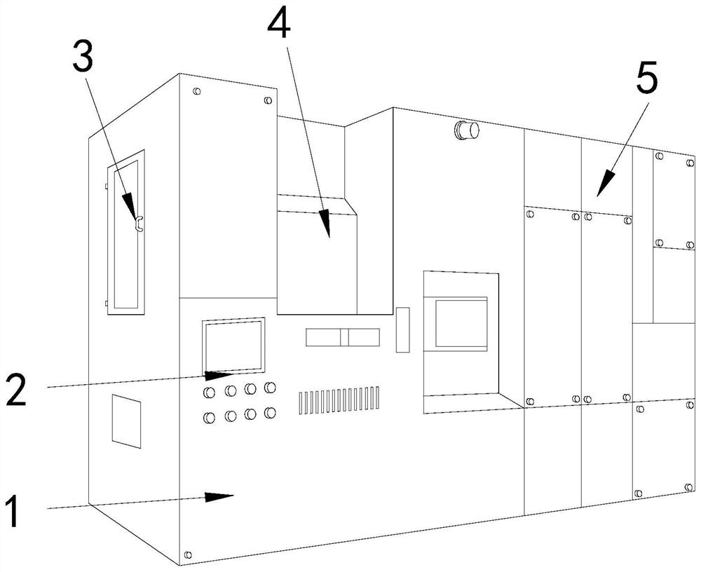
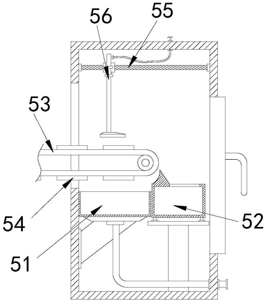

Embodiment 1

[0026] Example 1: Please refer to Figure 1-Figure 5 , the specific embodiments of the present invention are as follows:

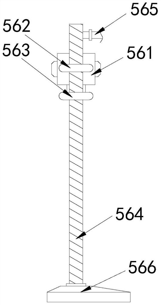
[0027] Its structure includes a main body 1, a control panel 2, a feed port 3, a photoresist block 4, and a developing device 5. The front end of the main body 1 is provided with a control panel 2, and the feed port 3 is arranged on the left side of the main body 1. The photoresist block 4 is located at one end of the main body 1, and the developing device 5 is arranged at the other end of the main body 1. The developing device 5 includes a photoresist recovery box 51, a wafer collection box 52, a conveyor belt 53, and a carrier plate 54 , a sliding rod 55, a material spraying device 56, the photoresist recovery box 51 is installed at one end of the bottom of the developing device 5, the wafer collection box 52 is installed at the other end of the bottom of the developing device 5, and the conveyor belt 53 is arranged on Just above the photoresist recover...

Embodiment 2

[0032] Example 2: Please refer to Figure 6-Figure 8 , the specific embodiments of the present invention are as follows:

[0033]The material blocking device a51 includes a carrier b1, a material blocking plate b2, a collecting tank b3, a cover plate b4, and a discharge head b5. The carrier b1 is cylindrical, and the material blocking plate b2 is provided with four uniform Arranged around the carrier b1, the collection tank b3 is set inside the material baffle b2, the cover plate b4 is engaged on the upper end of the collection tank b3, and the discharge head b5 is installed at the end of the collection tank b3 , the length of the cover plate b4 is shorter than the length of the collecting tank b3, which is beneficial to the removal and installation of the cover plate b4 in the collecting tank b3.

[0034] The cover plate b4 includes a collection hole b41, a feed head b42, a mounting groove b43, a return spring b44, and a block b45. There are more than five collection holes b...


PUM


Abstract

The invention discloses a wafer photoetching device. The photoetching device structurally comprises a main body, a control panel, a feeding hole, a photolithographic block and a developing device, wherein the feeding hole is formed in the left side of the main body, the developing device comprises a photoresist recycling box, a wafer collecting box, a conveying belt, a carrying disc, a sliding rodand a spraying device, the material spraying device comprises a transverse sliding block, a limiting block, a rotating block, a threaded rod, a material passing pipe and a discharging device, the discharging device comprises a material passing groove, a material spraying head, a groove, a power spraying head and a slag brushing device, the slag brushing device comprises a material blocking device, a rotating rod and a brush, and the material blocking device is arranged at a side end of the slag brushing device. The photoetching device is advantaged in that the power nozzle is used for vertically spraying the photoresist, the slag brushing device installed in the middle of the groove is impacted, the material blocking device is impacted to rotate, and therefore the brush fixedly embedded in the rotating rod rotates to brush residues on a surface of a wafer, and the situation that reacted residues are attached to the surface of the wafer, and development of the photoetching position ofthe post-reaction wafer is affected is avoided.

Description

technical field [0001] The invention relates to the field of wafer lithography and developing equipment, in particular to a wafer lithography equipment. Background technique [0002] Integrated circuit technology is the basic technology required by all electronic products today. The carrier of integrated circuit technology is the integrated circuit board. The most important part of the integrated circuit board is the wafer. The work of wafer lithography is extremely important, such as lithography Failure will directly lead to the scrapping of the wafer, which needs to be developed with a photoresist after photolithography. [0003] Based on the discovery by the inventors above, the existing wafer photolithography equipment mainly has the following disadvantages, such as: spraying the photoresist on the surface of the wafer, allowing the photoresist to chemically react with the wafer for development, The residue produced by the chemical reaction between the photoresist and t...

Claims


Application Information

Patent Timeline
Patent Type & Authority Applications(China)
IPC IPC(8): G03F7/30
CPCG03F7/30
Inventor 王涛
Owner 广州聪慧青贸易有限公司
Learn More