Touch assembly and touch display device

A touch component and touch layer technology, which is applied to instruments, electrical digital data processing, and data processing input/output processes, etc. problem, to achieve the effect of reducing impedance and increasing mutual capacitance

Pending Publication Date: 2020-10-02
WUHAN CHINA STAR OPTOELECTRONICS SEMICON DISPLAY TECH CO LTD
View PDF0 Cites 3 Cited by
  • Summary
  • Abstract
  • Description
  • Claims
  • Application Information

AI Technical Summary

Problems solved by technology

[0003] At present, the material of the touch electrode is usually a hollow metal mesh (Metal Mesh) material, and its conductive area is compared with the traditional full-surface transparent Indium Tin Oxide (Indium Tin Oxide, ITO) material touch electrode, and its actual effective conductive electrode The area is small, so the mutual capacitance between the driving electrode TX and the sensing electrode RX of the touch electrode is very small, resulting in a smaller capacitance change when touched by a finger, which is not easy to be detected by the touch chip (Touch IC) arrive
[0004] Therefore, it is necessary to propose a technical solution to solve the problem that the mutual capacitance between the driving electrode and the sensing electrode of the touch electrode is small

Method used


Image

  • Touch assembly and touch display device
  • Touch assembly and touch display device
  • Touch assembly and touch display device

Examples


Embodiment Construction

[0041] The technical solutions in the embodiments of the present application will be clearly and completely described below in conjunction with the drawings in the embodiments of the present application. Apparently, the described embodiments are only some of the embodiments of this application, not all of them. Based on the embodiments in this application, all other embodiments obtained by those skilled in the art without making creative efforts belong to the scope of protection of this application.

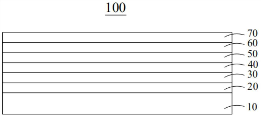
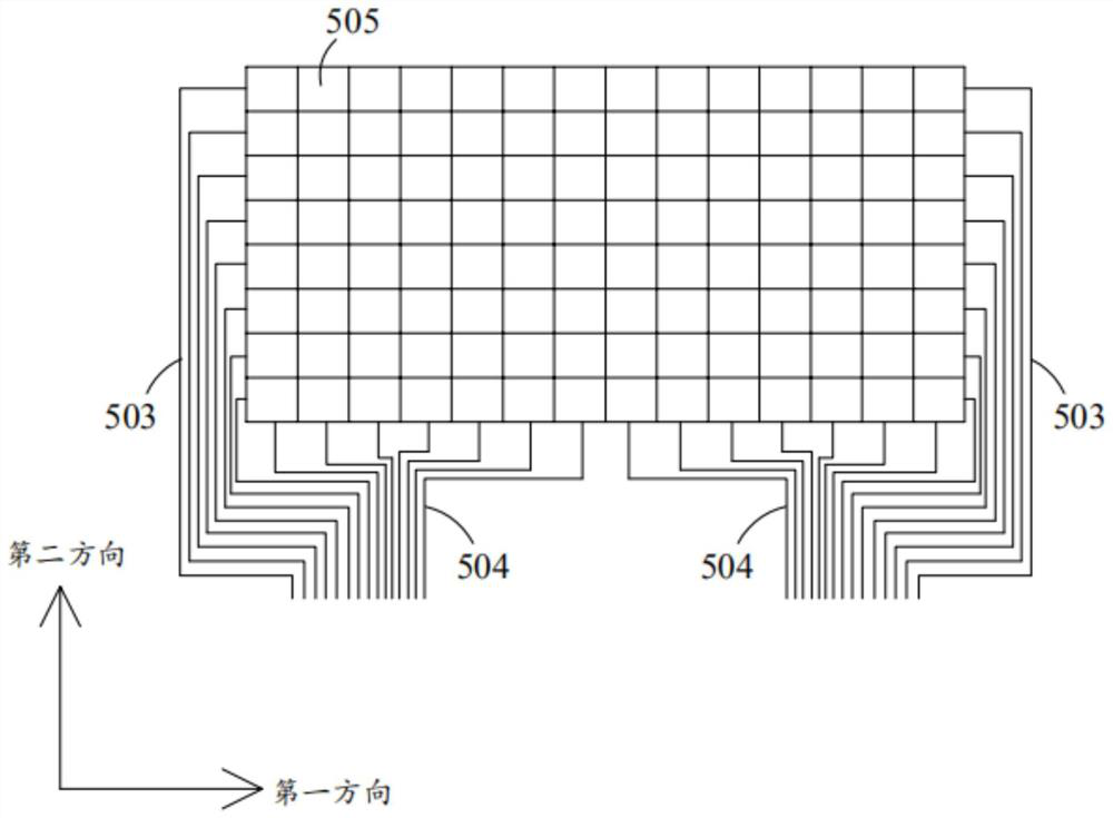
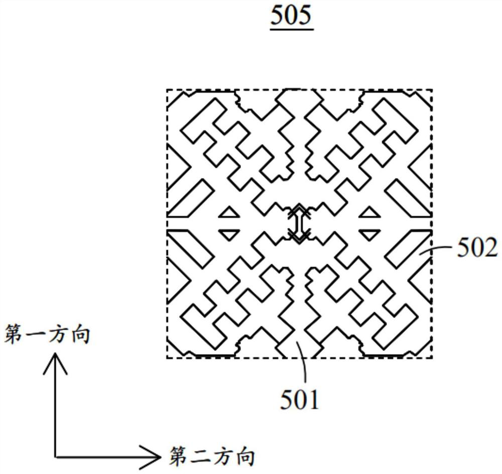
[0042] see figure 1, which is a schematic diagram of the touch display device of the present application. The touch display device can be a flexible and foldable touch display device, or a rigid touch display device. The touch display device includes a touch component and a display panel. The touch component can be located on one side of the display panel to form an add-on touch display device. The touch component can be located in the display panel to form an in-cell touch d...


PUM

PropertyMeasurementUnit
thicknessaaaaaaaaaa

Abstract

The invention provides a touch assembly and a touch display device. The touch control assembly comprises a touch control layer, the touch control layer comprises a plurality of touch control units, each touch control unit comprises a first touch control electrode arranged in the first direction, wherein each first touch control electrode comprises a first main electrode arranged in the first direction and at least one first branch electrode, and one end of each first branch electrode is electrically connected with the corresponding first main electrode; a second touch electrode which is arranged in the second direction, wherein the second touch control electrode comprises a second main electrode, at least one second branch electrode and at least one first connecting branch electrode whichare arranged along a second direction, one end of each second branch electrode is electrically connected with the second main electrode, the two ends of each first connecting branch electrode are electrically connected with the corresponding second branch electrode and the second main electrode respectively, the second branch electrodes surround the corresponding first branch electrodes, and the first direction is different from the second direction.

Description

technical field [0001] The present application relates to the field of touch technology, in particular to a touch component and a touch display device. Background technique [0002] Capacitive touch screens are widely used in various electronic interactive scene devices due to their high durability, long life, and support for multi-touch functions. The capacitive touch screen detects the specific position touched by the finger by detecting the change of capacitance at the position touched by the finger. [0003] At present, the material of the touch electrode is usually a hollow metal mesh (Metal Mesh) material, and its conductive area is compared with the traditional full-surface transparent Indium Tin Oxide (Indium Tin Oxide, ITO) material touch electrode, and its actual effective conductive electrode The area is small, so the mutual capacitance between the driving electrode TX and the sensing electrode RX of the touch electrode is very small, resulting in a smaller capac...

Claims


Application Information

Patent Timeline
Patent Type & Authority Applications(China)
IPC IPC(8): G06F3/044G06F3/041
CPCG06F3/0445G06F3/0412G06F3/0443G06F3/0448G06F3/0446G06F3/04164H10K59/40G06F2203/04111G06F2203/04112
Inventor 王杰平叶剑
Owner WUHAN CHINA STAR OPTOELECTRONICS SEMICON DISPLAY TECH CO LTD
Why Eureka
Try Eureka