Baffle design method for controlling film thickness distribution of ellipsoidal optical element

A technology of optical components and design methods, applied in the direction of ion implantation plating, coating, metal material coating process, etc.

Pending Publication Date: 2020-10-27
INST OF OPTICS & ELECTRONICS - CHINESE ACAD OF SCI
View PDF3 Cites 0 Cited by
  • Summary
  • Abstract
  • Description
  • Claims
  • Application Information

AI Technical Summary

Problems solved by technology

[0005] The technical problem to be solved by the present invention is: to overcome the deficiencies of the existing film thickness distribution model when the baffle is not used and the baffle design method for controlling the film thickness distribution on the ellipsoidal optical element in the vacuum coating process, respectively establish a real Reflect the thickness distribution model of the film deposited on the ellipsoidal optical element during the vacuum coating process without using the baffle and with the correction of the baffle, and provide an optimal design method of the baffle for controlling the thickness distribution of the film on the ellipsoidal optical element , to achieve precise control of film thickness distribution on ellipsoidal optical elements

Method used


Image

  • Baffle design method for controlling film thickness distribution of ellipsoidal optical element
  • Baffle design method for controlling film thickness distribution of ellipsoidal optical element
  • Baffle design method for controlling film thickness distribution of ellipsoidal optical element

Examples


Embodiment Construction

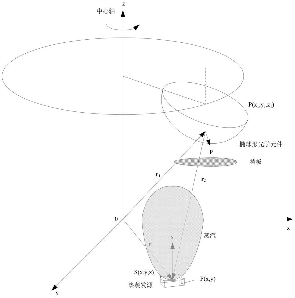
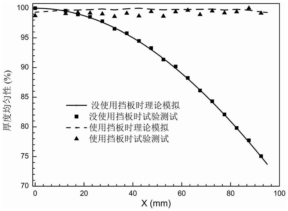
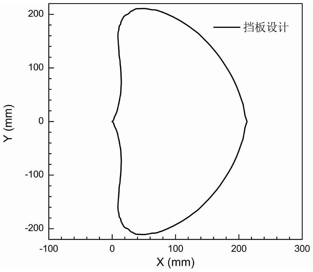
[0025] The principle of the present invention: the baffle control film thickness distribution technology is a method of using a baffle to selectively block the evaporated or sputtered film material during the vacuum coating process, so that the film thickness on the ellipsoidal optical element has a uniform distribution method. In the vacuum coating process, the evaporated or sputtered thin film material is transported in a vacuum environment and forms a thin film with non-uniform thickness distribution on the coating surface of the ellipsoidal optical element. The thickness distribution models of the film deposited on the ellipsoidal optical element during the vacuum coating process were established respectively when the baffle was not used and when the baffle was used for correction. Determine the evaporation or sputtering characteristics j of the thin film material in the vacuum coating process according to the film thickness distribution model when the baffle is not used. O...


PUM


Abstract

The invention discloses a baffle design method for controlling the film thickness distribution of an ellipsoidal optical element. A film material is transported in the vacuum coating process in a vacuum environment by evaporation or sputtering, and forms a film with non-uniform thickness distribution on the surface of the ellipsoidal optical element. Film thickness distribution models which can truly reflect the thickness distribution of the film deposited on the ellipsoidal optical element in the vacuum coating process when a baffle is not used and when the baffle is used for correction are respectively established. The evaporation or sputtering characteristics of the film material in the vacuum coating process are determined according to the film thickness distribution model when the baffle is not used; and on that basis, the film thickness distribution model when the baffle plate is used for correction is used for theoretically simulating the thickness distribution of the film deposited on the ellipsoidal optical element in the vacuum coating process. The baffle design is optimized by a computer until the film thickness distribution on the ellipsoidal optical element reaches thedesign requirements after the baffle is corrected; the optimal baffle design is obtained; and the precise control of the film thickness distribution on the ellipsoidal optical element can be realized.

Description

technical field [0001] The invention relates to the field of optical thin film element preparation, in particular to a baffle design method for controlling the film thickness distribution of an ellipsoidal optical element. Background technique [0002] The design of the optical system is becoming more and more sophisticated. In order to meet the performance indicators of the optical system, some optical systems use ellipsoidal optical elements, and special designed optical films are plated on the surface of the ellipsoidal optical elements to improve the performance of the ellipsoidal optical elements. The current techniques for preparing optical thin films on ellipsoidal optical elements can be mainly divided into physical vapor deposition (PVD) and chemical vapor deposition (CVD). Physical vapor deposition is a process in which a thin film is deposited on the surface of an ellipsoidal optical element by evaporating or sputtering a thin film material under vacuum conditions...

Claims


Application Information

Patent Timeline
Patent Type & Authority Applications(China)
IPC IPC(8): C23C14/54C23C14/24C23C14/34
CPCC23C14/542C23C14/24C23C14/34
Inventor 郭春孔明东
Owner INST OF OPTICS & ELECTRONICS - CHINESE ACAD OF SCI
Why Eureka
Try Eureka