Jig structure for semiconductor package and semiconductor package comprising same

A technology of semiconductors and structures, applied in semiconductor devices, semiconductor/solid-state device parts, electric solid-state devices, etc., can solve the problems of high cost and heavy weight of fixtures

Pending Publication Date: 2020-10-27
JMJ KOREA CO LTD
View PDF4 Cites 2 Cited by
  • Summary
  • Abstract
  • Description
  • Claims
  • Application Information

AI Technical Summary

Problems solved by technology

[0005] In addition, the existing jig structure is made of copper for welding, but there are pro

Method used


Image

  • Jig structure for semiconductor package and semiconductor package comprising same
  • Jig structure for semiconductor package and semiconductor package comprising same
  • Jig structure for semiconductor package and semiconductor package comprising same

Examples


Embodiment Construction

[0027] Hereinafter, preferred embodiments of the present invention will be described in detail with reference to the accompanying drawings. Moreover, in describing the present invention, when it is judged that the detailed description of related known functions or structures may unnecessarily obscure the gist of the present invention, the detailed description will be omitted.

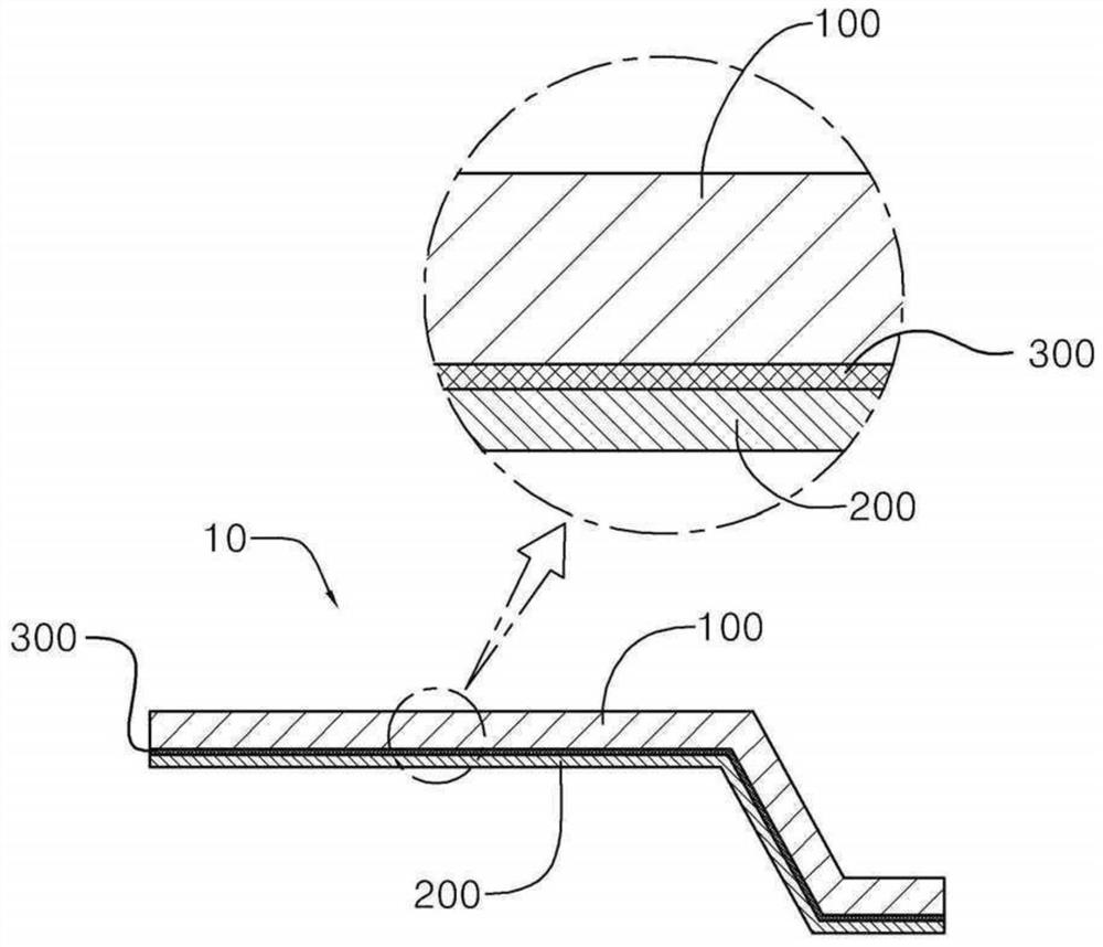
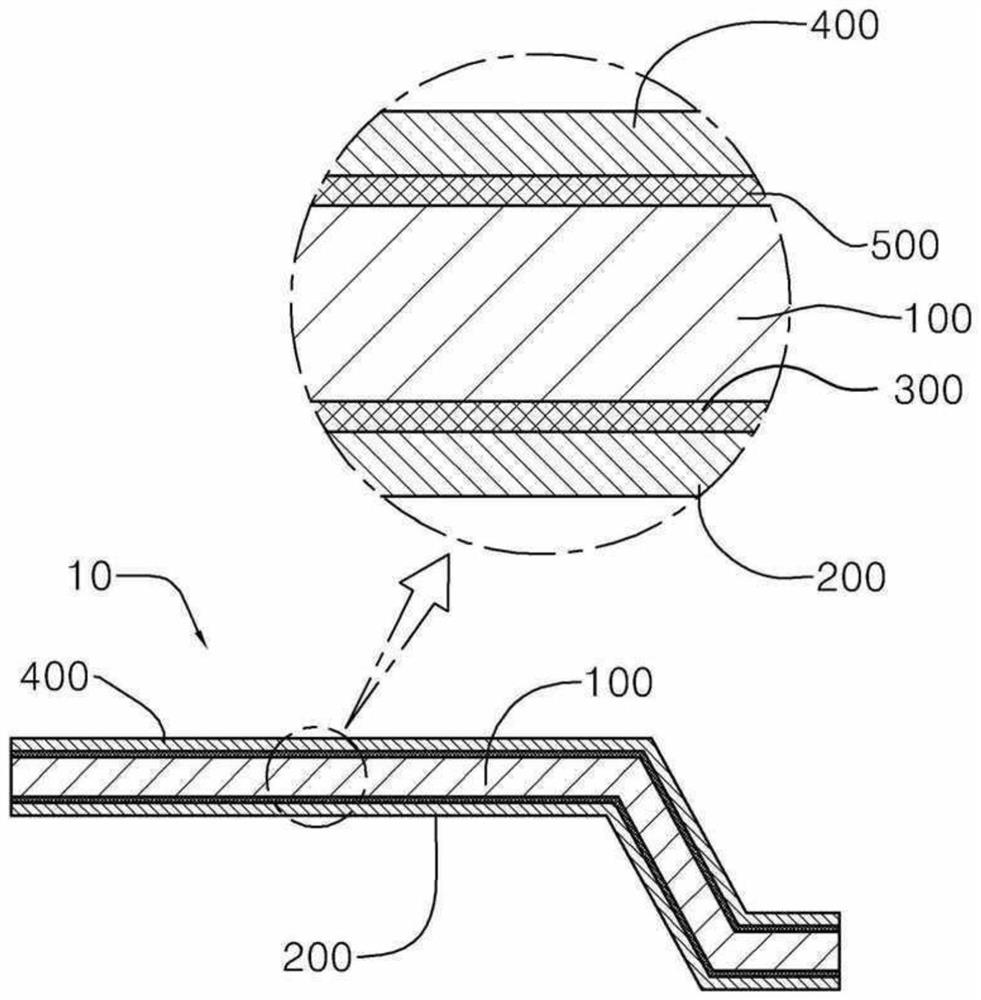
[0028] The jig structure 10 for electrically connecting the structure of the package in the semiconductor package of the present invention is characterized in that the structure of the jig structure 10 includes: a main metal layer 100 to maintain the shape of the jig structure 10; The functional layer 200 is stacked on one side of the main metal layer 100, and a metal different from the main metal layer 100 is used; the first bonding layer 300 is formed between the first functional layer 200 and the main metal layer 100, A metal that can bond the first functional layer 200 to the main metal layer 100 is...


PUM


Abstract

The present invention relates to a jig structure for a semiconductor package, and more specifically, to a jig structure suitable for a semiconductor package made of metal layers of different materials, instead of a single metal, thereby reducing the price of a semiconductor package manufactured by applying lightweight metal material at a low cost that would not be applicable in the past, and achieving a lightweight. That is, the jig structure for electrically connecting the structure of the package in the semiconductor package of the present invention is characterized in that the jig structureincludes: a main metal layer that maintains the shape of the jig structure; and a first functional layer that is laminated on one side of the main metal layer and suitable for a different type of metal from the main metal layer; and a first bonding layer that is formed between the first functional layer and the main metal layer, and is suitable for metal capable of bonding the first functional layer to the main metal layer.

Description

technical field [0001] The present invention relates to a jig structure for semiconductor packaging and a semiconductor package including the same. More specifically, it relates to a material of a jig structure suitable for semiconductor packaging that is composed of metal layers of different materials instead of a single metal, thereby reducing A light-weight jig structure for semiconductor packaging and a semiconductor package including the semiconductor package can be realized at the price of a semiconductor package manufactured by applying low-cost and light-weight metal, which was not available in the past. Background technique [0002] Generally, a semiconductor package includes a semiconductor chip, a lead frame, and a package body. The semiconductor chip is attached to pads of the lead frame, and the wires are bonded to pins of the lead frame to realize electrical connection. [0003] However, the conventional wire stack package realizes electrical signal exchange th...

Claims


Application Information

Patent Timeline
IPC IPC(8): H01L23/495H01L23/485
CPCH01L23/4951H01L23/49527H01L24/29H01L2224/29124H01L2224/29147H01L2224/40245H01L2224/48247H01L2224/73265H01L2924/181H01L2224/32245H01L2224/73221H01L2924/00012H01L2924/00H01L24/30H01L23/53209H01L24/06H01L23/528
Inventor 崔伦华金泳勋李泰宪赵廷焄
Owner JMJ KOREA CO LTD
Why Eureka
Try Eureka