Silicon-based deep ultraviolet avalanche photodiode and its preparation method
An avalanche photoelectric and deep ultraviolet technology, which is applied in circuits, electrical components, semiconductor devices, etc., can solve the problems of large lattice mismatch between AlN and GaN, and no one-dimensional deep ultraviolet avalanche diode is prepared, so as to improve the crystal quality and have a Facilitate the preparation and release of epitaxial stress
- Summary
- Abstract
- Description
- Claims
- Application Information
AI Technical Summary
Problems solved by technology
Method used
Image

Examples
Embodiment 1
[0040] First, take a piece of n-type Si substrate, and clean the surface of the Si substrate with HF acid, acetone and ethanol solution for 5 min respectively.
[0041] Then, the Si substrate is placed in a molecular beam epitaxy (Molecular beam epitaxy, MBE) growth chamber for epitaxial growth.
[0042] Specifically include the following steps:
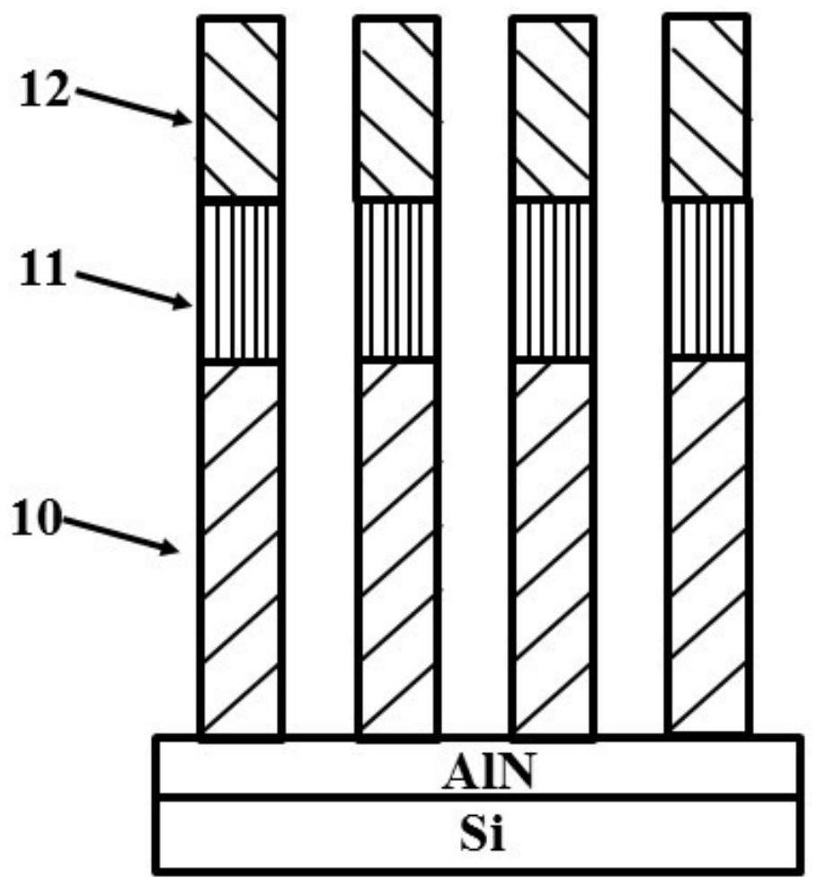
[0043] In the first step, an AlN buffer layer with a thickness of about 2 nm is grown on Si, such as figure 1 shown.
[0044] In the second step, a layer of highly doped (Si is the dopant source) n-type AlN nanocolumns 10 with a height of about 300 nm is grown on the AlN buffer layer to form the first AlN nanocolumns.
[0045] In the third step, a layer of unintentionally doped (i.e. low doped) Al with a thickness of 80 nm is grown on the first AlN nanocolumn. 0.5 Ga 0.5 N nano-column 11, re-grow a p-type AlN nano-column 12 with a thickness of 100nm of high doping (Mg is the dopant source); 1-m Ga m The value of m in the N nano...
Embodiment 2
[0048] First, take an n-type Si substrate, and clean the surface of the Si substrate with HF acid, acetone and ethanol solutions for 10 min respectively.
[0049] Then, the Si substrate was placed in an MBE growth chamber for epitaxial growth.
[0050] Specifically include the following steps:
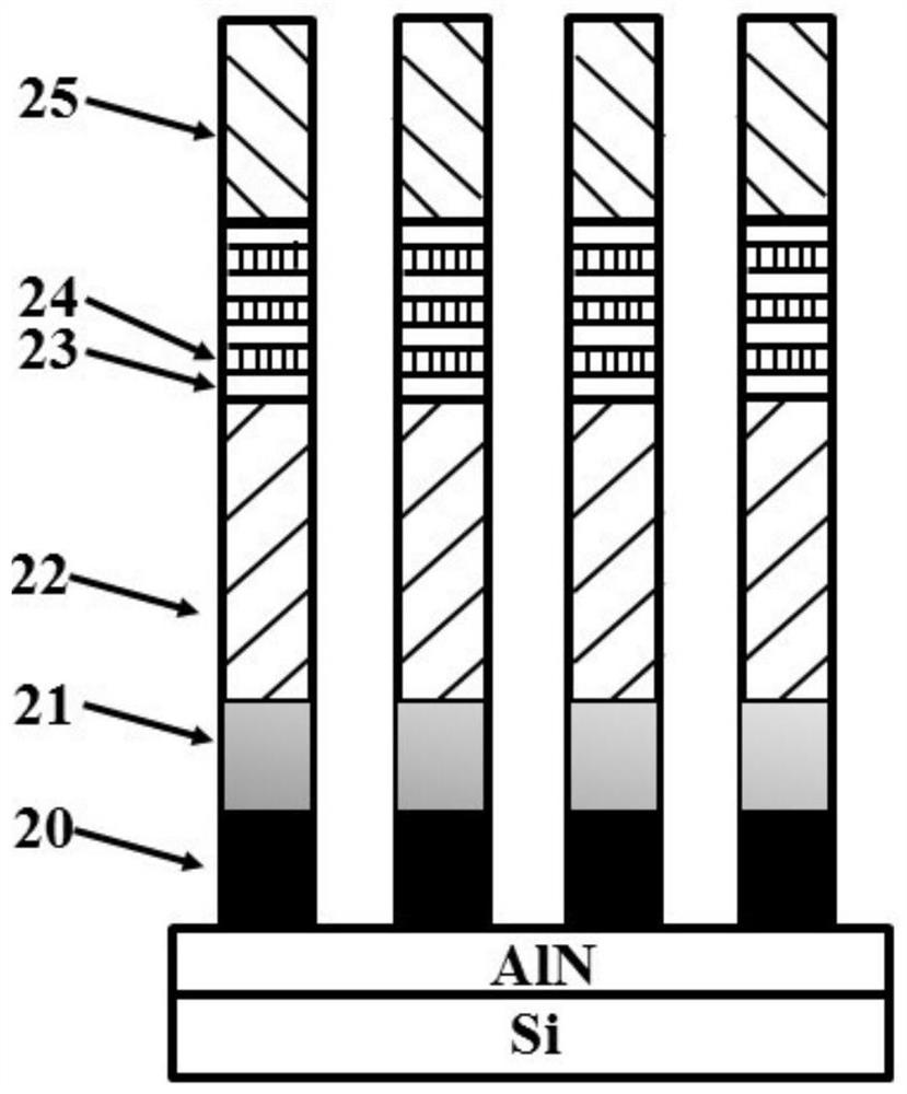
[0051] In the first step, an AlN buffer layer with a thickness of about 3 nm is grown on Si, such as figure 2 shown.
[0052] The second step is to grow a layer of highly Si-doped n-type GaN nanocolumns with a height of about 100 nm on the AlN buffer layer (the doping concentration is 5×10 19 / cm -3 )20, and then grow a layer of highly Si-doped Al with a height of 40nm 1-m Ga m N nanocolumns (doping concentration is 2×10 19 / cm -3 )21, in which the content of Al components increases gradually along the growth direction, and then grows a layer of highly Si-doped n-type AlN nanocolumns with a height of about 50 nm (doping concentration 3×10 19 / cm -3 )twenty two.
[0053] In t...
Embodiment 3
[0057] First, take an n-type Si substrate, and wash the surface of the Si substrate with acetone and ethanol solutions for 15 minutes respectively.
[0058] Then, the Si substrate was placed in an MBE growth chamber for epitaxial growth.
[0059] Specifically include the following steps:
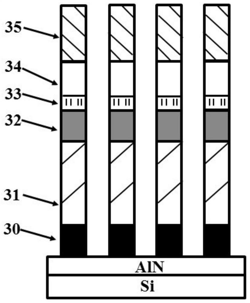
[0060] In the first step, an AlN buffer layer with a thickness of about 2 nm is grown on Si, such as image 3 shown.
[0061] In the second step, a layer of Si-doped n-type GaN nanocolumns 30 with a height of about 150 nm is grown on the AlN buffer layer, and then a layer of Si-doped Al with a height of 200 nm is grown. 0.4 Ga 0.6 N nanopillars 31 .
[0062] The third step is to grow a layer of unintentionally doped (ie low doped) Al with a thickness of 120nm. 0.55 Ga 0.45 N nanopillars 32 .
[0063] The fourth step is to grow a layer of Mg-doped p-type Al with a thickness of 60nm 0.5 Ga 0.5N nanopillars33.
[0064] In the fifth step, a layer of unintentionally doped Al with a thic...
PUM
| Property | Measurement | Unit |
|---|---|---|
| thickness | aaaaa | aaaaa |
| height | aaaaa | aaaaa |
| height | aaaaa | aaaaa |
Abstract
Description
Claims
Application Information
 - R&D Engineer
- R&D Manager
- IP Professional
- Industry Leading Data Capabilities
- Powerful AI technology
- Patent DNA Extraction
Browse by: Latest US Patents, China's latest patents, Technical Efficacy Thesaurus, Application Domain, Technology Topic.
© 2024 PatSnap. All rights reserved.Legal|Privacy policy|Modern Slavery Act Transparency Statement|Sitemap