Weak light spectrum detection chip and weak light spectrum detection method

A spectrum detection and weak light technology, applied in the field of spectrum equipment, can solve the problems of heavy cost, difficult operation and flexible movement, and large equipment volume

Pending Publication Date: 2020-10-30
TSINGHUA UNIV
View PDF0 Cites 2 Cited by
  • Summary
  • Abstract
  • Description
  • Claims
  • Application Information

AI Technical Summary

Problems solved by technology

For this reason, the present invention proposes a weak-light spectrum detection chip to solve the problem that the existing weak-light spectrum detection equipment relies too much on precision optical instruments, resulting in equipment that is too large, heavy and expensive, and is not easy to operate and move flexibly. The problem

Method used


Image

  • Weak light spectrum detection chip and weak light spectrum detection method
  • Weak light spectrum detection chip and weak light spectrum detection method
  • Weak light spectrum detection chip and weak light spectrum detection method

Examples


Embodiment 1

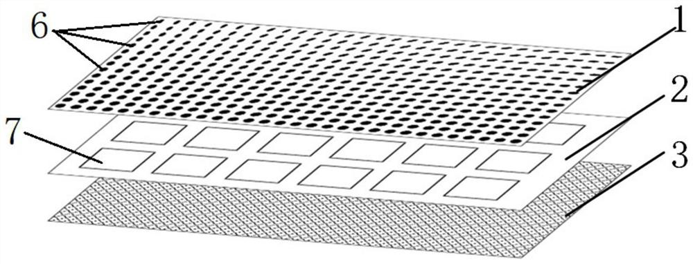
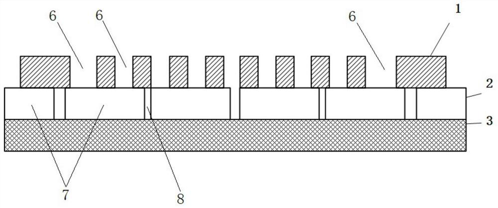
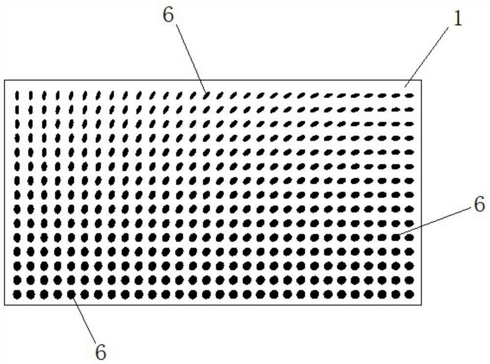
[0056] like figure 1 As shown, the first embodiment provides a weak light spectrum detection chip and a weak light spectrum detection method. In this chip, the light modulation layer 1 includes a modulation unit. All the modulation holes 6 in the modulation unit go through the bottom plate, such as figure 2 shown. All the modulation holes 6 in the modulation unit have the same cross-sectional shape, and the present embodiment uses figure 1 The ellipse is shown as an example. All the modulation holes 6 are arranged in an array in the light modulation layer 1 according to the order of the size of the structural parameters gradually changing, so as to form a two-dimensional pattern structure.

[0057] Specifically, in the two-dimensional graphic structure, all modulation holes 6 are arranged in an array, and all modulation holes 6 are arranged row by row and column by row according to the major axis length, minor axis length and rotation angle, so that all modulation The ho...

Embodiment 2

[0075] The structure and principle of the low-light spectrum detection chip described in the second embodiment, the weak-light spectrum detection method and the preparation method of the chip are basically the same as those in the first embodiment, and the similarities will not be repeated here. The difference is:

[0076] like Figure 6 As shown, in the chip described in this embodiment, an integral modulation unit is disposed on the light modulation layer 1 . Each modulation hole 6 in the two-dimensional graphic structure provided in the modulation unit has its own cross-sectional shape, and some modulation holes 6 have the same cross-sectional shape, but some modulation holes 6 have different cross-sectional shapes. Each modulation hole 6 is freely combined and arranged according to a specific cross-sectional shape. Specifically, in the two-dimensional graphic structure, each modulation hole 6 with the same cross-sectional shape constitutes a plurality of modulation hole ...

Embodiment 3

[0080] The structure, principle, weak light spectrum detection method and chip preparation method of the low-light spectrum detection chip described in the third embodiment are basically the same as those in the second embodiment, and the similarities will not be repeated here. The difference is:

[0081] like Figure 7 and Figure 8 As shown, two or more modulation units 5 are arranged on the light modulation layer 1 of this embodiment. In each modulation unit 5 , when the modulation holes 6 are combined and arranged according to a preset cross-sectional shape, the arrangement sequence is row by row or column by row according to a preset periodic sequence.

[0082] In this embodiment, all the modulation holes 6 are divided into several modulation units 5 according to different cross-sectional shapes, and the cross-sectional shapes of the modulation holes 6 in each modulation unit 5 are different from each other. The modulation holes 6 in the same modulation unit 5 have the...


PUM

PropertyMeasurementUnit
Thicknessaaaaaaaaaa
Areaaaaaaaaaaa
Thicknessaaaaaaaaaa

Abstract

The invention relates to the technical field of spectrum equipment, in particular to a weak light spectrum detection chip and a weak light spectrum detection method. The weak light spectrum detectionchip comprises a light modulation layer and a photoelectric detection layer, the light modulation layer comprises a bottom plate and at least one modulation unit, the bottom plate is horizontally arranged and connected onto the photoelectric detection layer, and a plurality of modulation holes penetrating through the bottom plate are formed in each modulation unit; the photoelectric detection layer comprises a plurality of groups of detection units, the detection units are arranged under the modulation unit, at least one photoelectric detector is arranged in each detection unit, and the photoelectric detectors are used for carrying out weak light detection on the modulated light after that incident light enters the modulation unit to form the modulated light, and obtaining a spectrum by reconstructing a response signal algorithm. According to the chip, a spectrograph is reduced to the chip level without depending on a precise optical instrument, the chip has the advantages of being stable in performance, low in cost, convenient to operate and carry and capable of moving flexibly, and spectral detection of weak light can be achieved.

Description

technical field [0001] The invention relates to the technical field of spectrum equipment, in particular to a weak light spectrum detection chip and a weak light spectrum detection method. Background technique [0002] The intensity of light is determined by the number of photons per unit area. The more photons, the stronger the light, and the fewer photons, the weaker the light. Currently, a spectrometer is an instrument for obtaining spectral information. The amount of information carried by the spectrum is rich, which is the objective and quantitative characteristics of light. At the same time, the measurement of the emission, absorption, and scattering spectra of substances can reveal the composition of substances from the molecular or even atomic level, and can be used in substance identification, detection and quantitative analysis. In some special application fields, it is often necessary to detect weak light due to reasons such as the protection of the measured obje...

Claims


Application Information

Patent Timeline
IPC IPC(8): G01J3/02G01J3/28
CPCG01J3/0243G01J3/2803G01J2003/2813G01J2003/2816G01J2003/282
Inventor 黄翊东崔开宇刘仿冯雪张巍
Owner TSINGHUA UNIV
Why Eureka
Try Eureka