Optical waveguide
A technology of optical waveguide and optical waveguide sheet, applied in the field of optical waveguide, can solve problems such as difficult to realize real-time detection and affect imaging quality, and achieve the effects of ensuring imaging quality, coupling efficiency, and coupling efficiency
- Summary
- Abstract
- Description
- Claims
- Application Information
AI Technical Summary
Problems solved by technology
Method used
Image
Examples
Embodiment 1
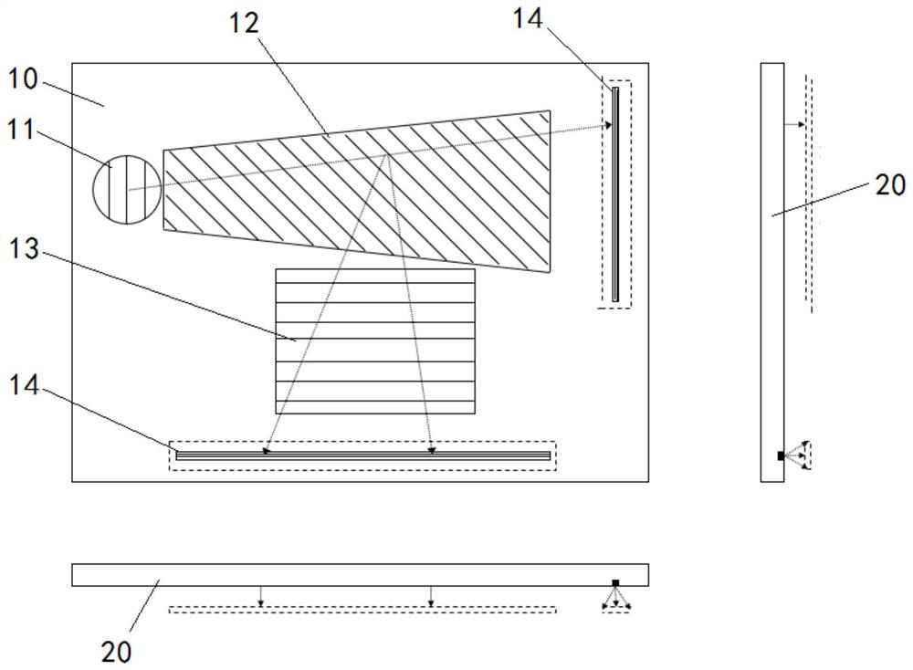
[0035] Such as figure 1 In the specific embodiment shown, the detector 20 is spaced apart from the optical waveguide sheet 10, and the optical waveguide further includes a plurality of slit gratings 14, and the slit gratings 14 are arranged on the optical waveguide sheet 10, and the slit gratings 14 and the detector 20 In one-to-one correspondence, the slit grating 14 is located in the light incident direction of the detector 20 . The slit grating 14 is arranged on the optical waveguide sheet 10, and the slit grating 14 is arranged in one-to-one correspondence with the detectors 20, and the slit grating 14 is located in the light incident direction of the detector 20, so that there is no outcoupling in the turning grating 12. Most of the light in the grating 13 and the light not used for imaging out of the grating 13 can enter the slit grating 14 and be coupled out from the slit grating 14 to the one-to-one corresponding detectors 20, which is convenient for the detector 20 to...
Embodiment 2
[0044] The difference from Embodiment 1 is that the position of the detector 20 is different.
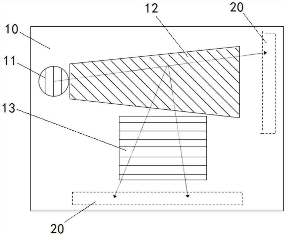
[0045] exist figure 2 In the specific embodiment shown, the slit grating 14 is not arranged on the optical waveguide 10 , and the detector 20 is arranged on the optical waveguide 10 . This setting makes the optical waveguide 10 and the detector 20 integrally formed, which facilitates the real-time detection of the light not used for imaging in the optical waveguide 10 by the detector 20, reduces the volume of the optical waveguide, and ensures the miniaturization of the optical waveguide. .
[0046] Such as figure 2 As shown, a plurality of detectors 20 are arranged on the same side surface of the optical waveguide plate 10 . When at least a part of the in-coupling grating 11, the inflection grating 12 and the out-coupling grating 13 are on the same surface, and multiple detectors 20 are arranged on the same side surface of the optical waveguide sheet 10, multiple detectors 20 ...
Embodiment 3
[0048] The difference from the second embodiment is that the position of the detector 20 is different.
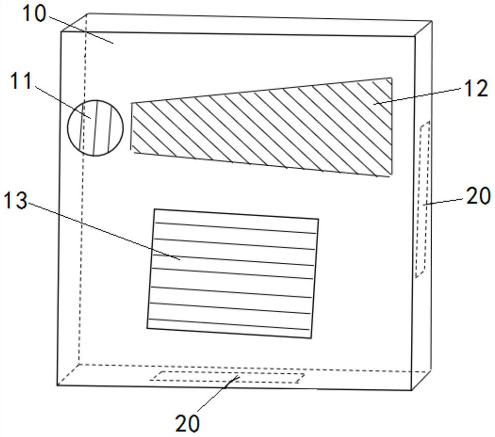
[0049] exist image 3 In the specific embodiment shown, at least two detectors 20 are arranged on different surfaces of the optical waveguide sheet 10 . The two detectors 20 are arranged on different surfaces of the optical waveguide sheet 10, so that the two detectors 20 receive light from different positions.
[0050] exist image 3 In the specific embodiment shown, at least a part of the coupling-in grating 11, the inflection grating 12 and the out-coupling grating 13 are on the same surface, and the two detectors 20 are respectively located on the same surface as the in-coupling grating 11, the inflection grating 12 and the out-coupling grating. 13 on both sides of the plane. exist image 3 In the specific embodiment shown, the optical waveguide 10 is a cuboid, the plane where the coupling-in grating 11, the turning grating 12 and the coupling-out grating 13 are loc...
PUM
| Property | Measurement | Unit |
|---|---|---|
| thickness | aaaaa | aaaaa |
| thickness | aaaaa | aaaaa |
Abstract
Description
Claims
Application Information


